AD7682 데이터 시트보기 (PDF) - Analog Devices
부품명
상세내역
일치하는 목록
AD7682 Datasheet PDF : 28 Pages
| |||
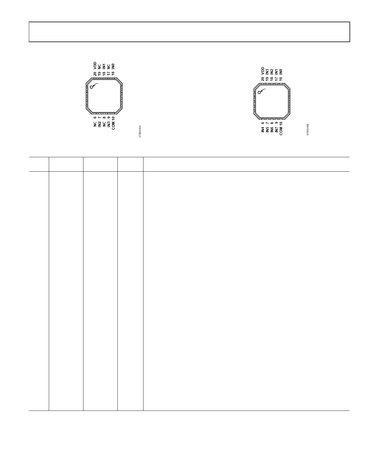
PIN CONFIGURATIONS AND FUNCTION DESCRIPTIONS
AD7682/AD7689
VDD 1
REF 2
REFIN 3
GND 4
GND 5
PIN 1
INDICATOR
AD7682
TOP VIEW
(Not to Scale)
15 VIO
14 SDO
13 SCK
12 DIN
11 CNV
VDD 1
REF 2
REFIN 3
GND 4
GND 5
PIN 1
INDICATOR
AD7689
TOP VIEW
(Not to Scale)
15 VIO
14 SDO
13 SCK
12 DIN
11 CNV
NC = NO CONNECT
Figure 4. AD7682 20-Lead LFCSP (QFN) Pin Configuration
Figure 5. AD7689 20-Lead LFCSP (QFN) Pin Configuration
Table 6. Pin Function Descriptions
Pin AD7682
AD7689
No. Mnemonic Mnemonic
1, 20 VDD
VDD
Type 1
P
2
REF
REF
AI/O
3
REFIN
REFIN
AI/O
4, 5 GND
GND
P
6
NC
IN4
AI
7
IN2
IN5
AI
8
NC
IN6
AI
9
IN3
IN7
AI
10 COM
COM
AI
11 CNV
CNV
DI
12 DIN
DIN
DI
13 SCK
SCK
DI
Description
Power Supply. Nominally 2.5 V to 5.5 V when using an external reference and decoupled
with 10 μF and 100 nF capacitors.
When using the internal reference for 2.5 V output, the minimum should be 2.7 V.
When using the internal reference for 4.096 V output, the minimum should be 4.5 V.
Reference Input/Output. See the Voltage Reference Output/Input section.
When the internal reference is enabled, this pin produces a selectable system
reference = 2.5 V or 4.096 V.
When the internal reference is disabled and the buffer is enabled, REF produces a
buffered version of the voltage present on the REFIN pin (VDD – 0.3 V maximum) useful
when using low cost, low power references.
For improved drift performance, connect a precision reference to REF (0.5 V to VDD).
For any reference method, this pin needs decoupling with an external 10 μF capacitor
connected as close to REF as possible. See the Reference Decoupling section.
Internal Reference Output/Reference Buffer Input. See the Voltage Reference
Output/Input section.
When using the internal reference, the internal unbuffered reference voltage is present
and needs decoupling with a 0.1μF capacitor.
When using the internal reference buffer, apply a source between 0.5 V and 4.096 V that
is buffered to the REF pin as described above.
Power Supply Ground.
AD7682: No connection.
AD7689: Analog Input Channel 4.
AD7682: Analog Input Channel 2.
AD7689: Analog Input Channel 5.
AD7682: No connection.
AD7689: Analog Input Channel 6.
AD7682: Analog Input Channel 3.
AD7689: Analog Input Channel 7.
Common Channel Input. All channels [3:0] or [7:0] can be referenced to a common mode
point of 0 V or VREF/2 V.
Convert Input. On the rising edge, CNV initiates the conversion. During conversion, if
CNV is held high, the busy indictor is enabled.
Data Input. This input is used for writing to the 14-bit configuration register. The
configuration register can be written to during and after conversion.
Serial Data Clock Input. This input is used to clock out the data on ADO and clock in data
on DIN in an MSB first fashion.
Rev. 0 | Page 9 of 28
Share Link: 