AD7641ACP 데이터 시트보기 (PDF) - Analog Devices
부품명
상세내역
일치하는 목록
AD7641ACP Datasheet PDF : 28 Pages
| |||
AD7641
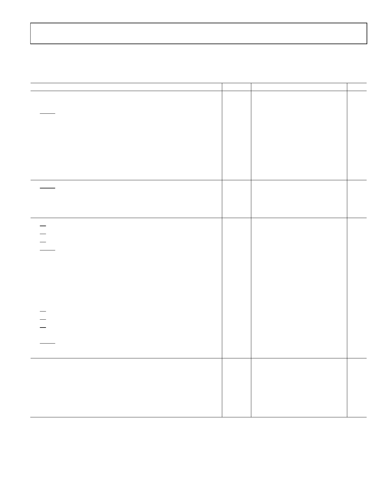
TIMING SPECIFICATIONS
AVDD = DVDD = 2.5 V; OVDD = 2.3 V to 3.6 V; VREF = 2.5 V; all specifications TMIN to TMAX, unless otherwise noted.
Table 3.
Parameter
CONVERSION AND RESET (Refer to Figure 29 and Figure 30)
Convert Pulse Width
Time Between Conversions (Warp Mode2/Normal Mode3)
CNVST Low to BUSY High Delay
BUSY High All Modes (Except Master Serial Read After Convert)
Aperture Delay
End of Conversion to BUSY Low Delay
Conversion Time (Warp Mode/Normal Mode)
Acquisition Time (Warp Mode/Normal Mode)
RESET Pulse Width
RESET Low to BUSY High Delay4
BUSY High Time from RESET Low4
PARALLEL INTERFACE MODES (Refer to Figure 31 to Figure 34 )
CNVST Low to Data Valid Delay (Warp Mode/Normal Mode)
Data Valid to BUSY Low Delay
Bus Access Request to Data Valid
Bus Relinquish Time
MASTER SERIAL INTERFACE MODES5 (Refer to Figure 35 and Figure 36)
CS Low to SYNC Valid Delay
CS Low to Internal SCLK Valid Delay5
CS Low to SDOUT Delay
CNVST Low to SYNC Delay (Warp Mode/Normal Mode)
SYNC Asserted to SCLK First Edge Delay
Internal SCLK Period6
Internal SCLK High6
Internal SCLK Low6
SDOUT Valid Setup Time6
SDOUT Valid Hold Time6
SCLK Last Edge to SYNC Delay6
CS High to SYNC HI-Z
CS High to Internal SCLK HI-Z
CS High to SDOUT HI-Z
BUSY High in Master Serial Read After Convert6
CNVST Low to SYNC Asserted Delay (All Modes)
SYNC Deasserted to BUSY Low Delay
SLAVE SERIAL INTERFACE MODES (Refer to Figure 38 and Figure 39)
External SCLK Setup Time
External SCLK Active Edge to SDOUT Delay
SDIN Setup Time
SDIN Hold Time
External SCLK Period
External SCLK High
External SCLK Low
Symbol Min
Typ
Max
Unit
t1
15
t2
500/667
t3
t4
t5
1
t6
10
t7
t8
115
t9
15
t38
10
t39
600
70 1
ns
ns
23
ns
385/520 ns
ns
ns
385/520 ns
ns
ns
ns
ns
t10
t11
2
t12
t13
2
385/520 ns
ns
20
ns
15
ns
t14
10
ns
t15
10
ns
t16
10
ns
t17
14/137
ns
t18
0.5
ns
t19
8
14
ns
t20
2
ns
t21
3
ns
t22
1
ns
t23
0
ns
t24
0
ns
t25
10
ns
t26
10
ns
t27
10
ns
t28
See Table 4
ns
t29
383/500
ns
t30
13
ns
t31
5
t32
1
t33
5
t34
5
t35
12.5
t36
5
t37
5
ns
8
ns
ns
ns
ns
ns
ns
1 See the Conversion Control section.
2 All timings for wideband warp mode are the same as warp mode.
3 In warp mode only, the maximum time between conversions is 1 ms; otherwise, there is no required maximum time.
4 See the Digital Interface section and the RESET section.
5 In serial interface modes, the SYNC, SCLK, and SDOUT timings are defined with a maximum load CL of 10 pF; otherwise, the load is 60 pF maximum.
6 In serial master read during convert mode. See Table 4 for serial master read after convert mode timing specifications.
Rev. 0 | Page 5 of 28
Share Link: 