EVAL-AD7291SDZ(Rev0) 데이터 시트보기 (PDF) - Analog Devices
부품명
상세내역
일치하는 목록
EVAL-AD7291SDZ Datasheet PDF : 28 Pages
| |||
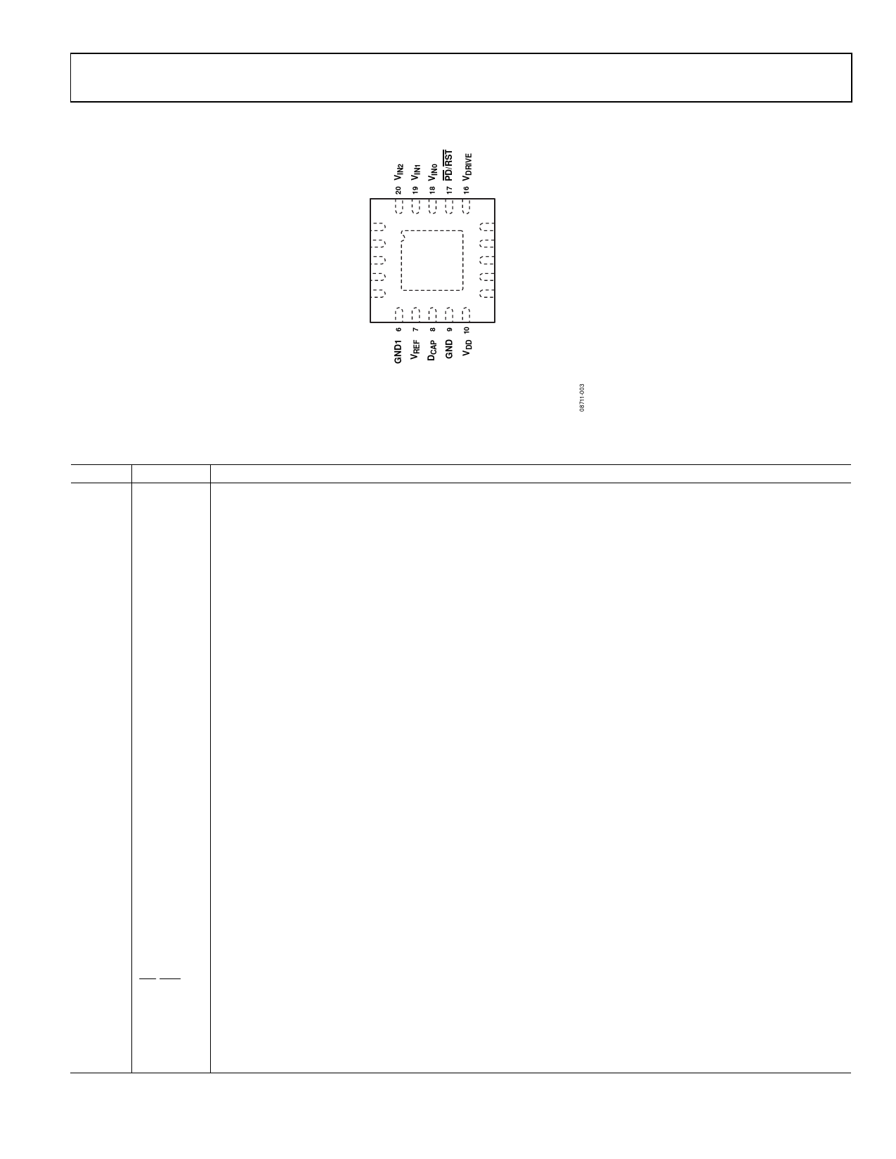
PIN CONFIGURATION AND FUNCTION DESCRIPTIONS
AD7291
VIN3 1
VIN4 2
VIN5 3
VIN6 4
VIN7 5
AD7291
TOP VIEW
(Not to Scale)
15 SCL
14 SDA
13 AS1
12 ALERT
11 AS0
NOTES
1. THE EXPOSED METAL PADDLE ON THE BOTTOM
OF THE LFCSP PACKAGE SHOULD BE SOLDERED
TO PCB GROUND FOR PROPER HEAT DISSIPATION
AND PERFORMANCE.
Figure 3. Pin Configuration
Table 6. Pin Function Descriptions
Pin No. Mnemonic Description
1 to 5,
18 to 20
6
VIN3, VIN4,
VIN5, VIN6,
VIN7, VIN0,
VIN1, VIN2
GND1
Analog Inputs. The AD7291 has eight single-ended analog inputs that are multiplexed into the on-chip track-and-
hold amplifier. Each input channel can accept analog inputs from 0 V to 2.5 V. Any unused input channels should
be connected to GND1 to avoid noise pickup.
Ground. Ground reference point for the internal reference circuitry on the AD7291. All analog input signals and
the external reference signals should be referred to this GND1 voltage. The GND1 pin should be connected to the
ground plane of a system. All ground pins should ideally be at the same potential and must not be more than 0.3 V
apart, even on a transient basis. The VREF pin should be decoupled to this ground pin via a 10 μF decoupling
capacitor.
7
VREF
8
DCAP
9
GND
10
11, 13
12
14
15
16
VDD
AS0, AS1
ALERT
SDA
SCL
VDRIVE
17
PD/RST
EPAD EPAD
Internal Reference/External Reference Supply. The nominal internal reference voltage of 2.5 V appears at this pin.
Provided the output is buffered, the on-chip reference can be taken from this pin and applied externally to the rest
of a system. Decoupling capacitors should be connected to this pin to decouple the reference buffer. For best
performance, it is recommended to use a 10 μF decoupling capacitor on this pin to GND1. The internal reference
can be disabled and an external reference supplied to this pin if required. The input voltage range for the external
reference is 2.0 V to 2.5 V.
Decoupling Capacitor Pin. Decoupling capacitors (1 μF recommended) are connected to this pin to decouple the
internal LDO.
Ground. Ground reference point for all analog and digital circuitry on the AD7291. The GND pin should be con-
nected to the ground plane of the system. All ground pins should ideally be at the same potential and must not be
more than 0.3 V apart, even on a transient basis. Both DCAP and VDD pins should be decoupled to this GND pin.
Supply Voltage, 2.8 V to 3.6 V. This supply should be decoupled to GND with 10 μF and 100 nF decoupling capacitors.
Logic Input. Together, the logic state of these two inputs selects a unique I2C address for the AD7291. See Table 31
for details. The device address depends on the voltage applied to these pins.
Digital Output. This pin acts as an out-of-range indicator and, if enabled, becomes active when the conversion
result violates the DATAHIGH or DATALOW register values. See the Limit Registers (0x04 to 0x1E) section.
Digital Input/Output. Serial bus bidirectional data. This open-drain output requires a pull-up resistor. The output coding
is straight binary for the voltage channels and twos complement for the temperature sensor result.
Digital Input. Serial I2C Bus Clock. This input requires a pull-up resistor. The data transfer rate in I2C mode is
compatible with both 100 kHz and 400 kHz operating modes.
Logic Power Supply Input. The voltage supplied at this pin determines the voltage at which the interface operates.
This pin should be decoupled to GND. The voltage range on this pin is 1.65 V to 3.6 V and may be less than the
voltage at VDD but should never exceed it by more than 0.3 V.
Power-Down Pin. This pin places the part into a full power-down mode and enables power conservation when
operation is not required. This pin can be used to reset the device by toggling the pin low for a minimum of 1 ns and a
maximum of 100 ns. If the maximum time is exceeded, the part enters power-down mode. When placing the device in
full power-down mode, the analog inputs must be returned to 0 V.
Exposed Paddle. The exposed metal paddle on the bottom of the LFCSP package should be soldered to PCB
ground for proper functionality and heat dissipation.
Rev. 0 | Page 7 of 28
Share Link: 