AD5744R(RevA) 데이터 시트보기 (PDF) - Analog Devices
부품명
상세내역
일치하는 목록
AD5744R
(Rev.:RevA)
(Rev.:RevA)
Analog Devices

AD5744R Datasheet PDF : 32 Pages
| |||
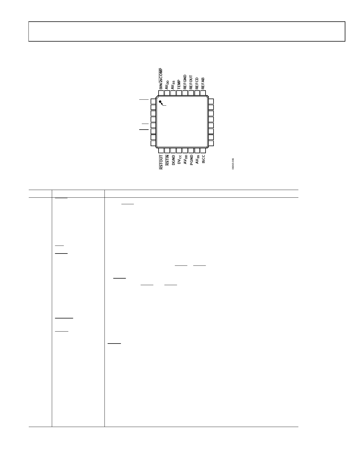
PIN CONFIGURATION AND FUNCTION DESCRIPTIONS
AD5744R
32 31 30 29 28 27 26 25
SYNC 1
SCLK 2
SDIN 3
SDO 4
CLR 5
LDAC 6
D0 7
D1 8
PIN 1
AD5744R
TOP VIEW
(Not to Scale)
24 AGNDA
23 VOUTA
22 VOUTB
21 AGNDB
20 AGNDC
19 VOUTC
18 VOUTD
17 AGNDD
9 10 11 12 13 14 15 16
Figure 6. Pin Configuration
Table 6. Pin Function Descriptions
Pin No. Mnemonic Description
1
SYNC
Active Low Input. This is the frame synchronization signal for the serial interface. While SYNC is low, data is transferred
in on the falling edge of SCLK.
2
SCLK
Serial Clock Input. Data is clocked into the shift register on the falling edge of SCLK. This operates at clock
speeds of up to 30 MHz.
3
SDIN
Serial Data Input. Data must be valid on the falling edge of SCLK.
4
SDO
Serial Data Output. This pin is used to clock data from the serial register in daisy-chain or readback mode.
5
CLR
Negative Edge Triggered Input.1 Asserting this pin sets the DAC registers to 0x0000.
6
LDAC
Load DAC. This logic input is used to update the DAC registers and, consequently, the analog outputs. When
tied permanently low, the addressed DAC register is updated on the rising edge of SYNC. If LDAC is held high
during the write cycle, the DAC input register is updated, but the output update is held off until the falling edge
of LDAC. In this mode, all analog outputs can be updated simultaneously on the falling edge of LDAC. The LDAC
pin must not be left unconnected.
7, 8
D0, D1
9
RSTOUT
Digital I/O Port. D0 and D1 form a digital I/O port. The user can set up these pins as inputs or outputs that are
configurable and readable over the serial interface. When configured as inputs, these pins have weak internal
pull-ups to DVCC. When programmed as outputs, D0 and D1 are referenced by DVCC and DGND.
Reset Logic Output. This is the output from the on-chip voltage monitor used in the reset circuit. If desired, it
can be used to control other system components.
10
RSTIN
Reset Logic Input. This input allows external access to the internal reset logic. Applying a Logic 0 to this input clamps
the DAC outputs to 0 V. In normal operation, RSTIN should be tied to Logic 1. Register values remain unchanged.
11
DGND
Digital Ground Pin.
12
DVCC
Digital Supply Pin. Voltage ranges from 2.7 V to 5.25 V.
13, 31 AVDD
Positive Analog Supply Pins. Voltage ranges from 11.4 V to 16.5 V.
14
PGND
Ground Reference Point for Analog Circuitry.
15, 30
16
AVSS
ISCC
Negative Analog Supply Pins. Voltage ranges from –11.4 V to –16.5 V.
This pin is used in association with an optional external resistor to AGND to program the short-circuit current of
the output amplifiers. Refer to the Design Features section for more information.
17
AGNDD
Ground Reference Pin for DAC D Output Amplifier.
18
VOUTD
Analog Output Voltage of DAC D. Buffered output with a nominal full-scale output range of ±10 V. The output
amplifier is capable of directly driving a 10 kΩ, 200 pF load.
19
VOUTC
Analog Output Voltage of DAC C. Buffered output with a nominal full-scale output range of ±10 V. The output
amplifier is capable of directly driving a 10 kΩ, 200 pF load.
20
AGNDC
Ground Reference Pin for DAC C Output Amplifier.
21
AGNDB
Ground Reference Pin for DAC B Output Amplifier.
22
VOUTB
Analog Output Voltage of DAC B. Buffered output with a nominal full-scale output range of ±10 V. The output
amplifier is capable of directly driving a 10 kΩ, 200 pF load.
Rev. A | Page 11 of 32
Share Link: