AD5429 데이터 시트보기 (PDF) - Analog Devices
부품명
상세내역
일치하는 목록
AD5429 Datasheet PDF : 32 Pages
| |||
AD5429/AD5439/AD5449
TIMING CHARACTERISTICS
VDD = 2.5 V to 5.5 V, VREF = 5 V, IOUT2 = 0 V. All specifications TMIN to TMAX, unless otherwise noted.
See Figure 2 and Figure 3. Temperature range for Y version is −40°C to +125°C. Guaranteed by design and characterization, not subject to
production test. All input signals are specified with tr = tf = ns (10% to 90% of VDD) and timed from a voltage level of (VIL + VIH)/2.
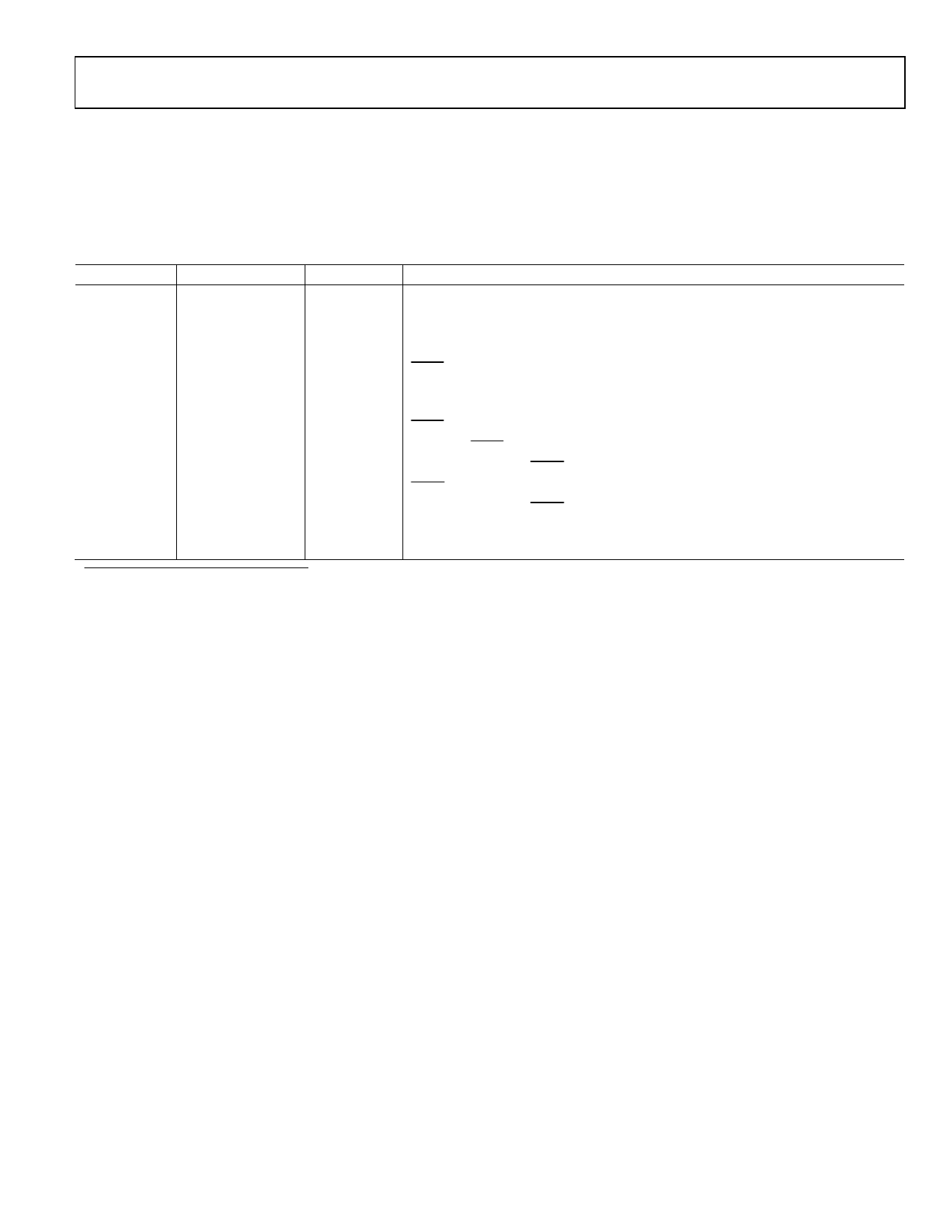
Table 2.
Parameter
fSCLK
t1
t2
t3
t4
t5
t6
t7
t8
t9
t10
t11
t122
Limit at TMIN, TMAX
50
20
8
8
13
5
4
5
30
0
12
10
25
60
Unit
MHz max
ns min
ns min
ns min
ns min
ns min
ns min
ns min
ns min
ns min
ns min
ns min
ns min
ns min
Conditions/Comments1
Max clock frequency
SCLK cycle time
SCLK high time
SCLK low time
SYNC falling edge to SCLK falling edge setup time
Data setup time
Data hold time
SYNC rising edge to SCLK falling edge
Minimum SYNC high time
SCLK falling edge to LDAC falling edge
LDAC pulse width
SCLK falling edge to LDAC rising edge
SCLK active edge to SDO valid, strong SDO driver
SCLK active edge to SDO valid, weak SDO driver
1 Falling or rising edge as determined by the control bits of the serial word. Strong or weak SDO driver selected via the control register.
2 Daisy-chain and readback modes cannot operate at maximum clock frequency. SDO timing specifications are measured with a load circuit, as shown in Figure 4.
Rev. 0 | Page 5 of 32
Share Link: 