AD2S105 데이터 시트보기 (PDF) - Analog Devices
부품명
상세내역
일치하는 목록
AD2S105 Datasheet PDF : 12 Pages
| |||
AD2S105
PIN DESIGNATIONS1, 2, 3
Pin
Mnemonic
Description
3
4
5
6
7
10
11
12
13
14
15
16
17
19
20
21
22
23
24
25
26
27–38
41
42
44
STROBE
VDD
VSS
PH/OP4
PH/OP1
AGND
PH/IP4
PH/IPH3
PH/IP3
PH/IPH2
PH/IP2
PH/IPH1
PH/IP1
VSS
HPREF
HPOP
HPFILT
CONV1
CONV2
COS
SIN
DB12 to DB1
VDD
DGND
BUSY
Begin Conversion
Positive Power Supply
Negative Power Supply
Sin (θ + φ)
Cos (θ + φ)
Analog Ground
Sin θ Input
High Level Cos
(θ + 240°) Input
Cos (θ + 240°) Input
High Level Cos
(θ + 120°) Input
Cos (θ + 120°) Input
High Level Cos θ Input
Cos (θ) Input
Negative Power Supply
Homopolar Reference
Homopolar Output
Homopolar Filter
Select Analog Input
Format
Select Analog Input
Format
Cos Output
Sin Output
(DB1 = MSB, DB12 =
LSB Parallel Input Data)
Positive Power Supply
Digital Ground
Internal Logic Setup
Time
NOTES
190° orthogonal signals = Sin θ, Cos θ (Resolver) = PH/IP4 and PH/IP1.
2Three phase, 120°, three-wire signals = Cos θ, Cos (θ + 120°), Cos (θ + 240°).
= PH/IP1, PH/IP2, PH/IP3
High Level = PH/IPH1, PH/IPH2, PH/IPH3.
3Three Phase, 120°, two-wire signals = Cos (θ + 120°), Cos (θ + 240°) =
PH/IP2, PH/IP3.
In all cases where any of the input Pins 11 through 17 are not used, they must
be left unconnected.
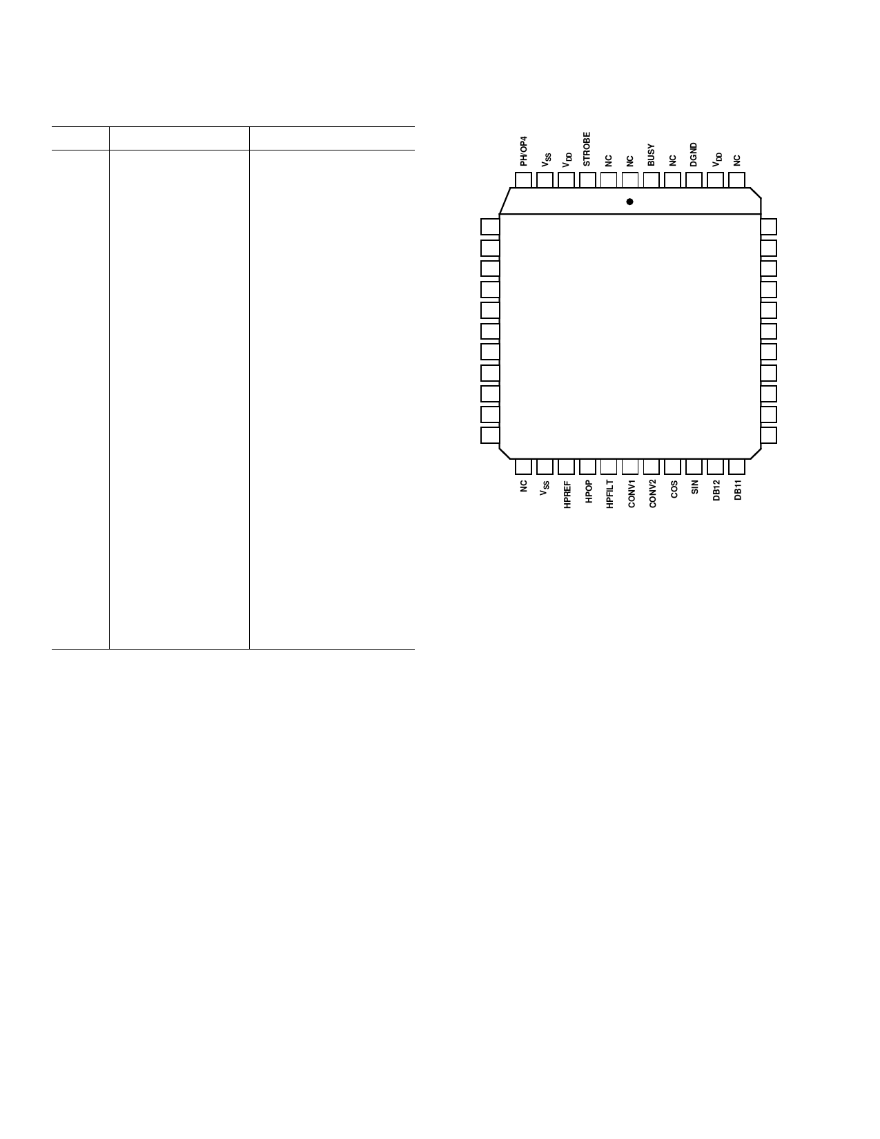
PIN CONFIGURATION
6 5 4 3 2 1 44 43 42 41 40
PH/OP1 7
NC 8
NC 9
AGND 10
PH/IP4 11
PH/IPH3 12
PH/IP3 13
PH/IPH2 14
PH/IP2 15
PH/IPH1 16
PH/IP1 17
AD2S105
TOP VIEW
(NOT TO SCALE)
39 NC
38 DB1
37 DB2
36 DB3
35 DB4
34 DB5
33 DB6
32 DB7
31 DB8
30 DB9
29 DB10
18 19 20 21 22 23 24 25 26 27 28
NC = NO CONNECT.
–4–
REV. 0
Share Link: 