AD1985JSTZ 데이터 시트보기 (PDF) - Analog Devices
부품명
상세내역
일치하는 목록
AD1985JSTZ Datasheet PDF : 48 Pages
| |||
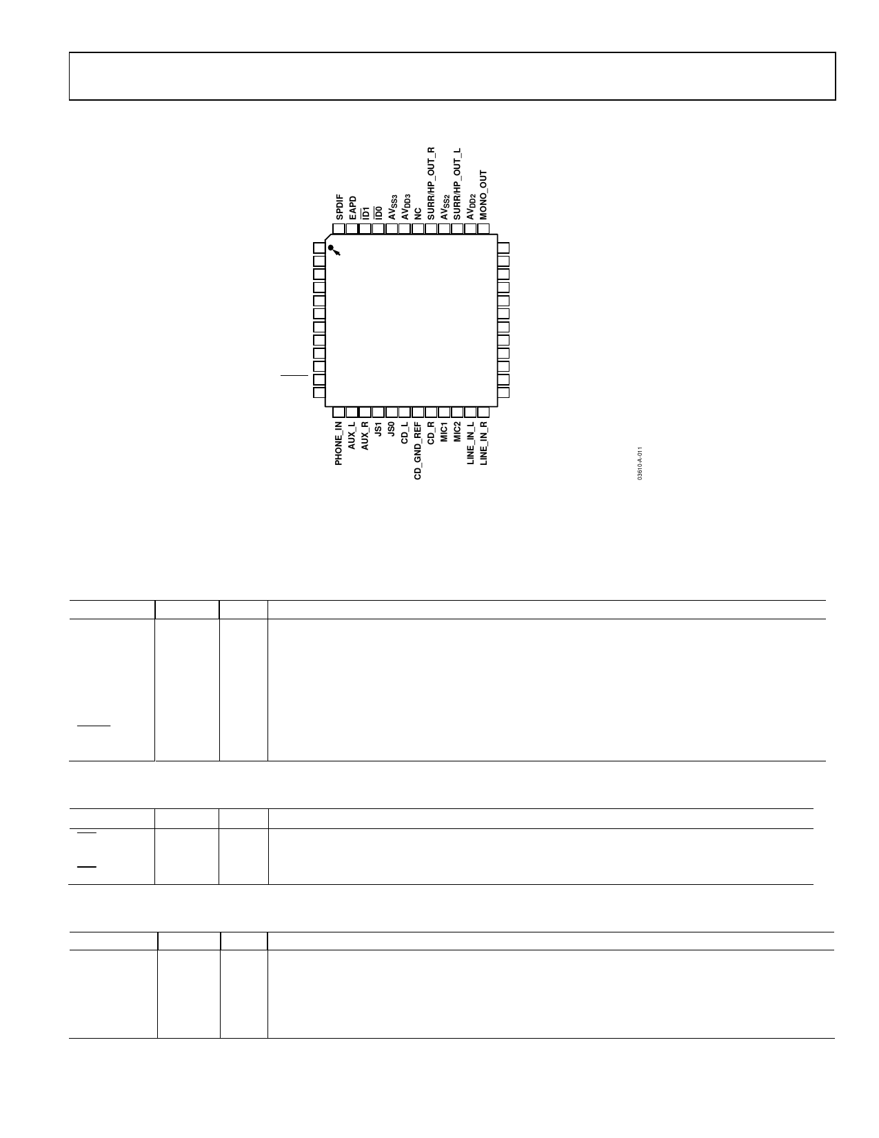
PIN CONFIGURATION AND FUNCTION DESCRIPTIONS
AD1985
48 47 46 45 44 43 42 41 40 39 38 37
DVDD1 1
XTL_IN 2
XTL_OUT 3
DVSS1 4
SDATA_OUT 5
BIT_CLK 6
DVSS2 7
SDATA_IN 8
DVDD2 9
SYNC 10
RESET 11
JS3 12
PIN 1
IDENTIFIER
AD1985
TOP VIEW
(Not to Scale)
36 LINE_OUT_R (FRONT)/SURR_R
35 LINE_OUT_L (FRONT)/SURR_L
34 AVDD4
33 JS2
32 LFE_OUT
31 CENTER_OUT
30 AFILT2
29 AFILT1
28 VREFOUT
27 VREF
26 AVSS1
25 AVDD1
13 14 15 16 17 18 19 20 21 22 23 24
NC = NO CONNECT
Figure 10. 48-Lead LQFP Pin Configuration
Circuit Layout Note: In normal operation, Surround and Line Out are swapped to provide headphone drive on line outputs. Therefore, Pins 35 and 36 become the
surround L/R outputs and Pins 39 and 41 become the Line Out (Front) L/R outputs with headphone drive. See Bits LOSEL and HPSEL in Register 0x76 for details.
PIN FUNCTION DESCRIPTIONS
Table 17. Digital I/O
Mnemonic Pin No. I/O Description
XTL_IN
2
I
Crystal Input (24.576 MHz) or External Clock In (24.576 MHz, 14.31818 MHz, or 48.000 MHz).
XTL_OUT
3
O
Crystal Output.
SDATA_OUT 5
I
AC Link Serial Data Output. AD1985 input stream.
BIT_CLK
6
O/I AC Link Bit Clock. 12.288 MHz serial data clock. (Input pin, for secondary mode only.)
SDATA_IN 8
O
AC Link Serial Data Input. AD1985 output stream.
SYNC
10
I
AC Link Frame Sync.
RESET
11
I
AC Link Reset. AD1985 master hardware reset.
SPDIF
48
O
SPDIF Output.
Table 18. Chip Selects/Clock Strapping
Mnemonic Pin No. I/O Description
ID0
45
I
Chip Select Input 0 (Active Low).
This pin can also be used as the chain input from a secondary codec.
ID1
46
I
Chip Select Input 1 (Active Low).
Table 19. Jack Sense/EAPD
Mnemonic Pin No. Type
EAPD
47
O
JS0
17
I
JS1
16
I
JS2
33
I
JS3
12
I
Description
EAPD Output.
JACK SENSE 0 Input.
JACK SENSE 1 Input.
JACK SENSE 2 Input.
JACK SENSE 3 Input.
Rev. A | Page 11 of 48
Share Link: 