AD1886A 데이터 시트보기 (PDF) - Analog Devices
부품명
상세내역
일치하는 목록
AD1886A Datasheet PDF : 28 Pages
| |||
AD1886A
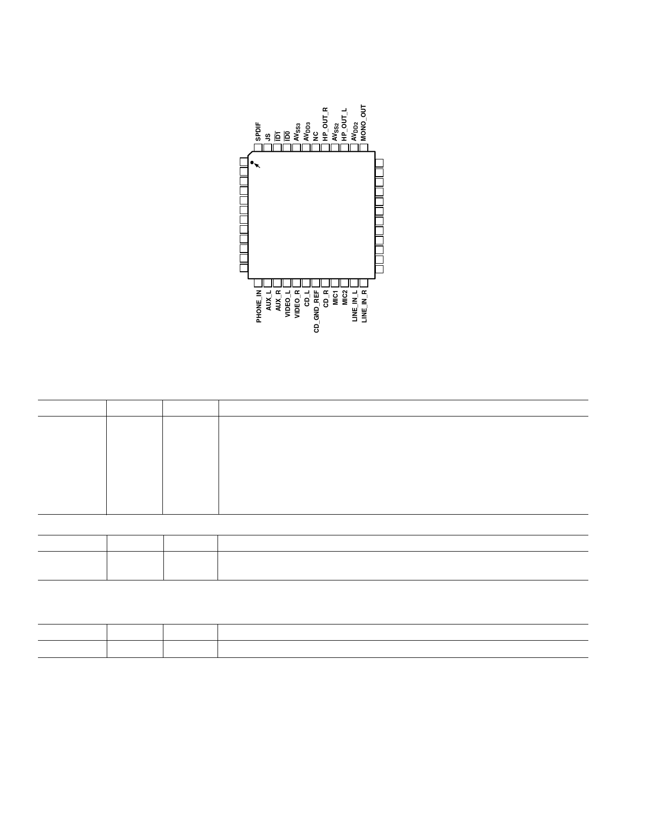
PIN CONFIGURATION
48 47 46 45 44 43 42 41 40 39 38 37
DVDD1 1
XTL_IN 2
XTL_OUT 3
DVSS1 4
SDATA_OUT 5
BIT_CLK 6
DVSS2 7
SDATA_IN 8
DVDD2 9
SYNC 10
RESET 11
PC_BEEP 12
PIN 1
IDENTIFIER
AD1886A
TOP VIEW
(Not to Scale)
13 14 15 16 17 18 19 20 21 22 23 24
36 LINE_OUT_R
35 LINE_OUT_L
34 CX3D
33 RX3D
32 FILT_L
31 FILT_R
30 AFILT2
29 AFILT1
28 VREFOUT
27 VREF
26 AVSS1
25 AVDD1
NC = NO CONNECT
PIN FUNCTION DESCRIPTIONS
Digital I/O
Pin Name
LQFP
I/O
XTL_IN
2
I
XTL_OUT
3
O
SDATA_OUT 5
I
BIT_CLK
6
O/I
SDATA_IN
8
O
SYNC
RESET
10
I
11
I
SPDIF
48
O
Description
Crystal (or Clock) Input, 24.576 MHz.
Crystal Output
AC-Link Serial Data Output, AD1886A Input Stream.
AC-Link Bit Clock. 12.288 MHz Serial Data Clock. Daisy-Chain Output Clock.
AC-Link Serial Data Input. AD1886A Output Stream.
AC-Link Frame Sync
AC-Link Reset. AD1886A Master H/W Reset.
SPDIF Output
CHIP SELECTS
Pin Name
LQFP
ID0
45
ID1
46
Type
I
I
Description
Chip Select Input 0 (Active Low)
Chip Select Input 1 (Active Low)
JACK SENSE/GENERAL-PURPOSE DIGITAL OUTPUT
The JS pin can be used to sense the presence of an audio plug in the output jacks and automatically mute the MONO and/or
LINE_OUT audio outputs. Alternatively, the JS can be programmed as a general-purpose digital output pin.
Pin Name
LQFP
Type
Description
JS
47
I/O
JACK SENSE Input, or GPIO.
–8–
REV. 0
Share Link: 