74VHCT00AN 데이터 시트보기 (PDF) - Fairchild Semiconductor
부품명
상세내역
일치하는 목록
74VHCT00AN Datasheet PDF : 6 Pages
| |||
July 1997
Revised March 1999
74VHCT00A
Quad 2-Input NAND Gate
General Description
The VHCT00A is an advanced high-speed CMOS 2-Input
NAND Gate fabricated with silicon gate CMOS technology.
It achieves the high-speed operation similar to equivalent
Bipolar Schottky TTL while maintaining the CMOS low
power dissipation. The internal circuit is composed of 3
stages, including buffer output, which provide high noise
immunity and stable output.
Protection circuits ensure that 0V to 7V can be applied to
the input pins without regard to the supply voltage and to
the output pins with VCC = 0V. These circuits prevent
device destruction due to mismatched supply and input/
output voltages. This device can be used to interface 3V to
5V systems and two supply systems such as battery
backup.
Features
s High speed: tPD = 5.0 ns (typ) at TA = 25°C
s High noise immunity: VIH = 2.0V, VIL = 0.8V
s Power down protection is provided on all inputs and
outputs
s Low noise: VOLP = 0.8V (max)
s Low power dissipation:
ICC = 2 µA (max) at TA = 25°C
s Pin and function compatible with 74HCT00
Ordering Code:
Order Number Package Number
Package Description
74VHCT00AM
M14A
14-Lead Small Outline Integrated Circuit (SOIC), JEDEC MS-120, 0.150 Narrow
74VHCT00ASJ
74VHCT00AMTC
74VHCT00AN
M14D
MTC14
N14A
14-Lead Small Outline Package (SOP), EIAJ TYPE II, 5.3mm Wide
14-Lead Thin Shrink Small Outline Package (TSSOP), JEDEC MO-153, 4.4mm Wide
14-Lead Plastic Dual-In-Line Package (PDIP), JEDEC MS-001, 0.300 Wide
Surface mount packages are also available on Tape and Reel. Specify by appending the suffix letter “X” to the ordering code.
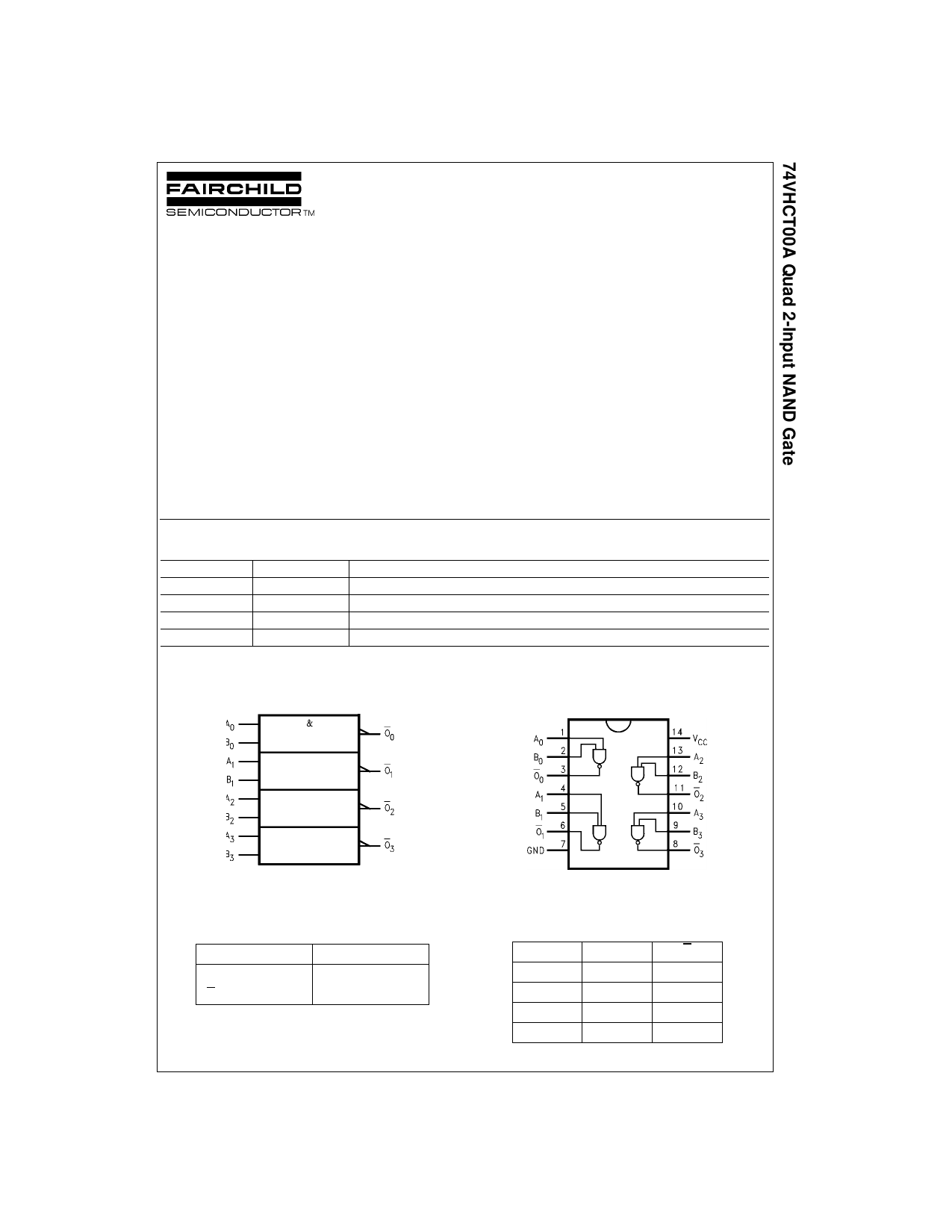
Logic Symbol
Connection Diagram
Pin Descriptions
Pin Names
An, Bn
On
Description
Inputs
Outputs
Truth Table
A
L
L
H
H
© 1999 Fairchild Semiconductor Corporation DS500023.prf
B
O
L
H
H
H
L
H
H
L
www.fairchildsemi.com
Share Link: 