74LVC1G126GF 데이터 시트보기 (PDF) - Nexperia B.V. All rights reserved
부품명
상세내역
일치하는 목록
74LVC1G126GF Datasheet PDF : 19 Pages
| |||
Nexperia
74LVC1G126
Bus buffer/line driver; 3-state
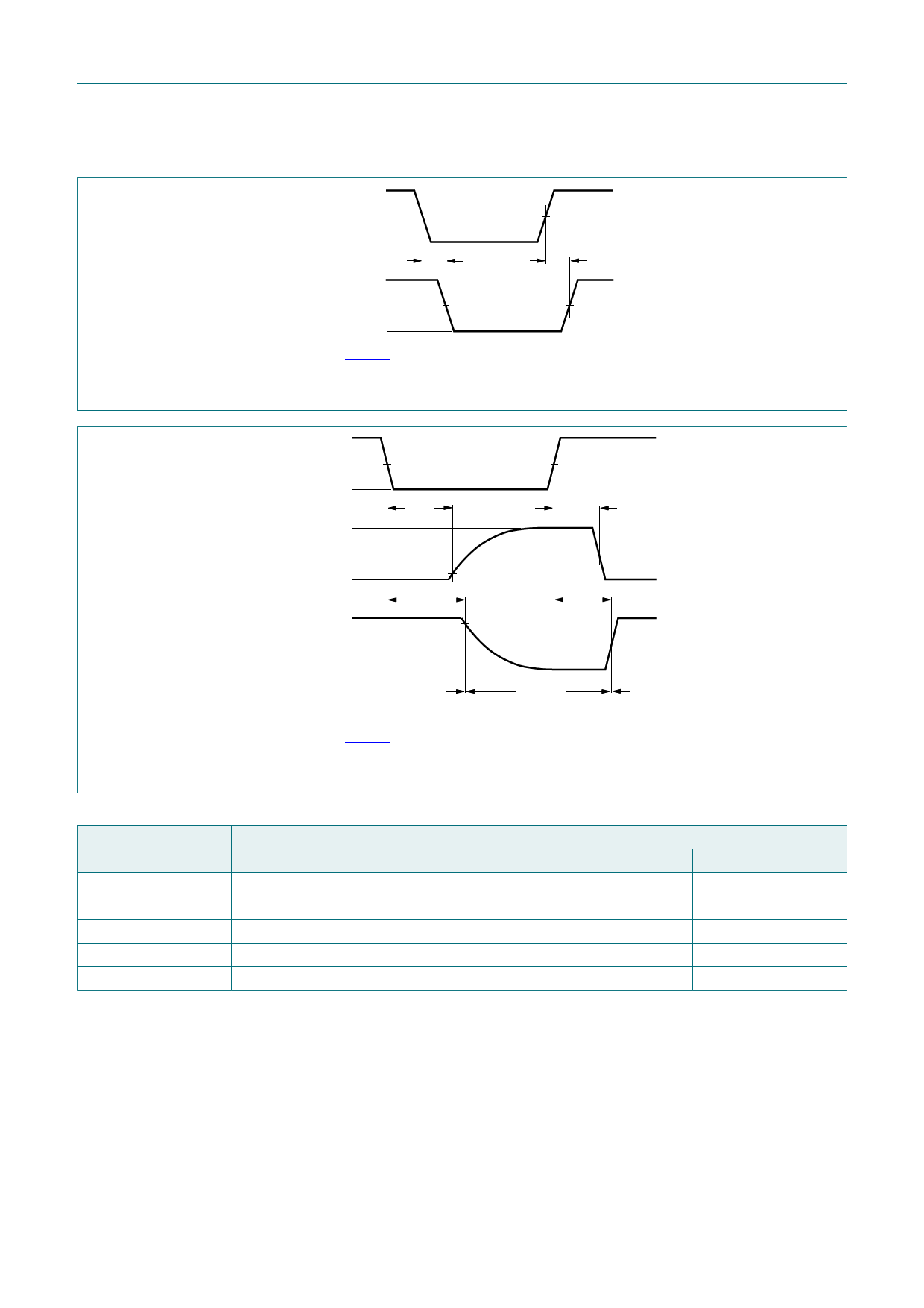
11.1. Waveforms and test circuit
VI
A input
VM
GND
VOH
tPHL
t PLH
Y output
VM
Fig. 8.
VOL
mnb153
Measurement points are given in Table 9.
VOL and VOH are typical output voltage levels that occur with the output load.
Input A to output Y propagation delay times
VI
OE input
VM
Fig. 9.
GND
tPLZ
tPZL
VCC
output
LOW-to-OFF
OFF-to-LOW
VOL
VOH
output
HIGH-to-OFF
OFF-to-HIGH
GND
tPHZ
VX
VY
output
enabled
VM
tPZH
output
disabled
VM
output
enabled
mna646
Measurement points are given in Table 9.
VOL and VOH are typical output voltage levels that occur with the output load.
3-state enable and disable times
Table 9. Measurement points
Supply voltage
Input
VCC
1.65 V to 1.95 V
VM
0.5VCC
2.3 V to 2.7 V
0.5VCC
2.7 V
1.5 V
3.0 V to 3.6 V
1.5 V
4.5 V to 5.5 V
0.5VCC
Output
VM
0.5VCC
0.5VCC
1.5 V
1.5 V
0.5VCC
VX
VOL + 0.15 V
VOL + 0.15 V
VOL + 0.3 V
VOL + 0.3 V
VOL + 0.3 V
VY
VOH - 0.15 V
VOH - 0.15 V
VOH - 0.3 V
VOH - 0.3 V
VOH - 0.3 V
74LVC1G126
Product data sheet
All information provided in this document is subject to legal disclaimers.
Rev. 14 — 15 March 2019
© Nexperia B.V. 2019. All rights reserved
8 / 19
Share Link: 