74LVC1G126GV 데이터 시트보기 (PDF) - Nexperia B.V. All rights reserved
부품명
상세내역
일치하는 목록
74LVC1G126GV Datasheet PDF : 19 Pages
| |||
Nexperia
74LVC1G126
Bus buffer/line driver; 3-state
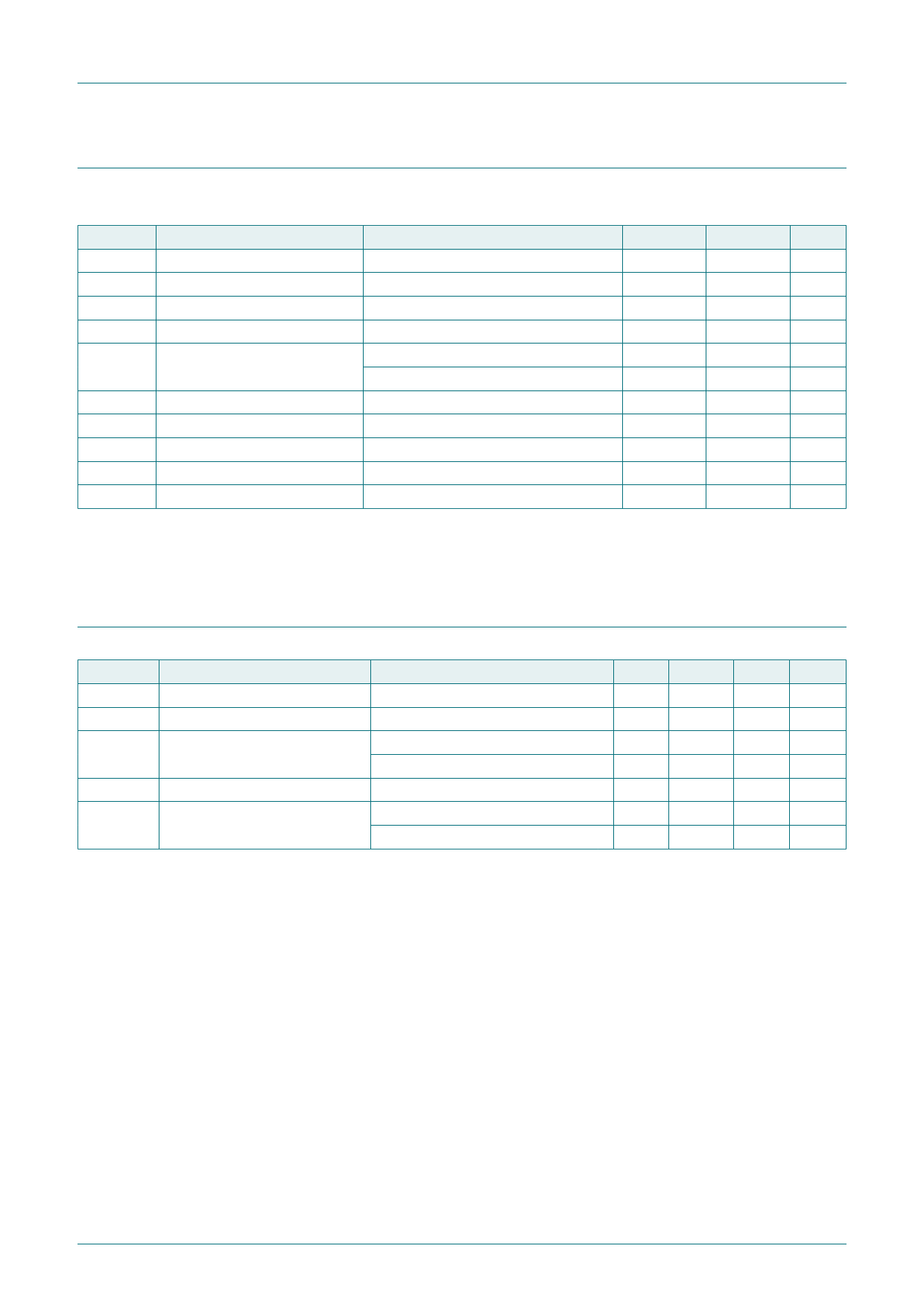
8. Limiting values
Table 5. Limiting values
In accordance with the Absolute Maximum Rating System (IEC 60134). Voltages are referenced to GND (ground = 0 V).
Symbol Parameter
Conditions
Min
Max Unit
VCC
IIK
VI
IOK
VO
IO
ICC
IGND
Ptot
Tstg
supply voltage
input clamping current
input voltage
output clamping current
output voltage
output current
supply current
ground current
total power dissipation
storage temperature
VI < 0 V
VO > VCC or VO < 0 V
Active mode
Power-down mode; VCC = 0 V
VO = 0 V to VCC
Tamb = -40 °C to +125 °C
-0.5
-50
[1] -0.5
-
[1] -0.5
[1] -0.5
-
-
-100
[2]
-
-65
+6.5 V
-
mA
+6.5 V
±50 mA
VCC + 0.5 V
+6.5 V
±50 mA
100 mA
-
mA
250 mW
+150 °C
[1] The input and output voltage ratings may be exceeded if the input and output current ratings are observed.
[2] For TSSOP5 and SC-74A packages: above 87.5 °C the value of Ptot derates linearly with 4.0 mW/K.
For XSON6 and X2SON5 package: above 118 °C the value of Ptot derates linearly with 7.8 mW/K.
9. Recommended operating conditions
Table 6. Recommended operating conditions
Symbol Parameter
Conditions
VCC
supply voltage
VI
input voltage
VO
output voltage
Active mode
VCC = 0 V; Power-down mode
Tamb
ambient temperature
Δt/ΔV
input transition rise and fall rate VCC = 1.65 V to 2.7 V
VCC = 2.7 V to 5.5 V
Min
Typ
Max Unit
1.65
-
5.5 V
0
-
5.5 V
0
-
VCC V
0
-
5.5 V
-40
-
+125 °C
-
-
20 ns/V
-
-
10 ns/V
74LVC1G126
Product data sheet
All information provided in this document is subject to legal disclaimers.
Rev. 14 — 15 March 2019
© Nexperia B.V. 2019. All rights reserved
4 / 19
Share Link: 