74LV367 데이터 시트보기 (PDF) - Philips Electronics
부품명
상세내역
일치하는 목록
74LV367 Datasheet PDF : 12 Pages
| |||
Philips Semiconductors
Hex buffer/line driver (3-State)
Product specification
74LV367
FEATURES
• Optimized for Low Voltage applications: 1.0 to 3.6V
• Accepts TTL input levels between VCC = 2.7V and VCC = 3.6V
• Typical VOLP (output ground bounce) t 0.8V @ VCC = 3.3V,
Tamb = 25°C
• Typical VOHV (output VOH undershoot) u 2V @ VCC = 3.3V,
Tamb = 25°C
• Non-inverting outputs
• Output capability: bus driver
• ICC category: MSI
DESCRIPTION
The 74LV367 is a low-voltage CMOS device and is pin and function
compatible 74HC/HCT367.
The 74LV367 is a hex non-inverting buffer/line driver with 3-State
outputs. The 3-State outputs (nY) are controlled by the output
enable inputs (1OE, 2OE).
A HIGH on nOE, causes the outputs to assume a high impedance
OFF-state.
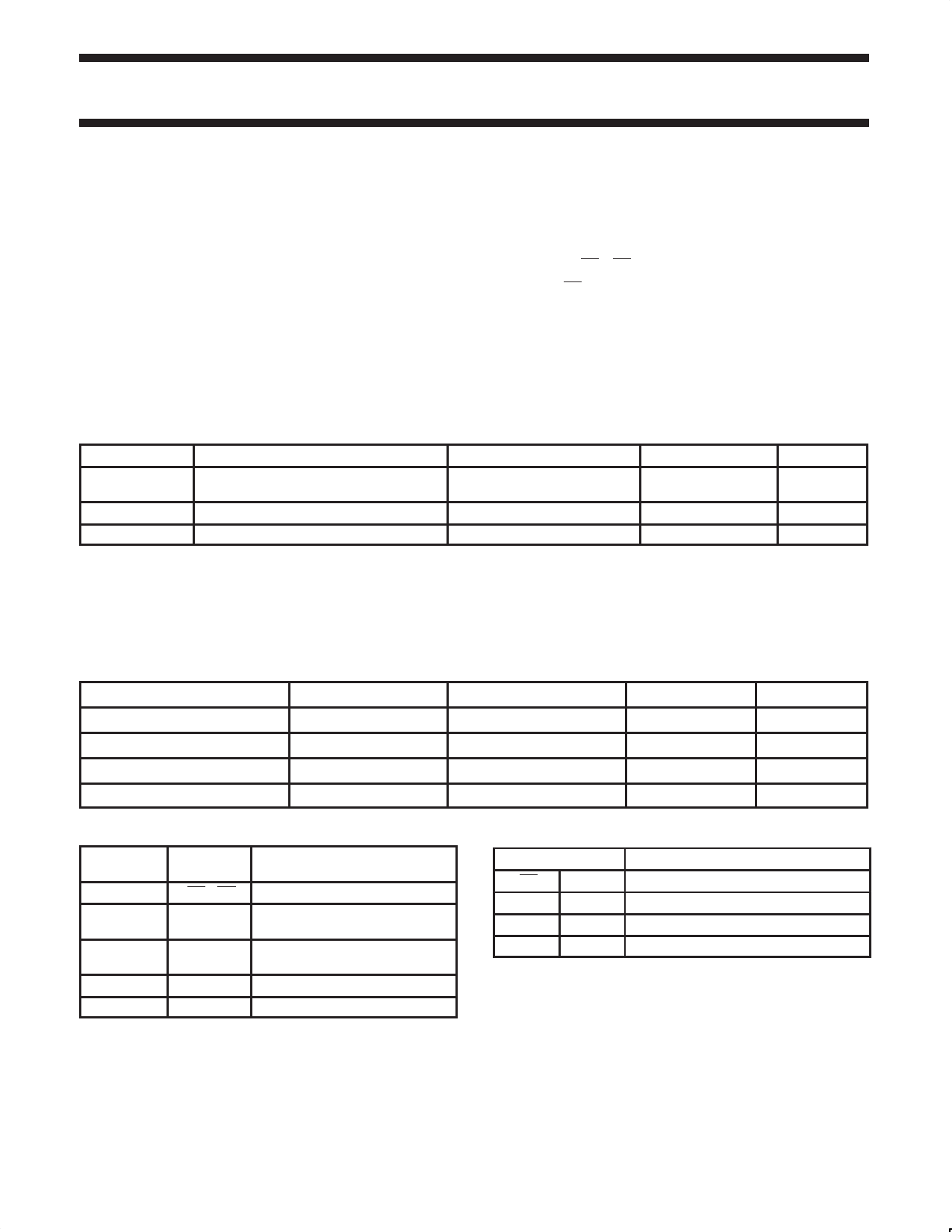
QUICK REFERENCE DATA
GND = 0V; Tamb = 25°C; tr = tf v2.5 ns
SYMBOL
PARAMETER
CONDITIONS
tPHL/tPLH
Propagation delay
nA to nY
CL = 15pF
VCC = 3.3V
CI
Input capacitance
CPD
Power dissipation capacitance per buffer Notes 1 and 2
NOTES:
1. CPD is used to determine the dynamic power dissipation (PD in µW)
PD = CPD VCC2 fi )S (CL VCC2 fo) where:
fi = input frequency in MHz; CL = output load capacitance in pF;
fo = output frequency in MHz; VCC = supply voltage in V;
S (CL VCC2 fo) = sum of the outputs.
2. The condition is VI = GND to VCC
TYPICAL
8
3.5
30
ORDERING INFORMATION
PACKAGES
16-Pin Plastic DIL
16-Pin Plastic SO
16-Pin Plastic SSOP Type II
16-Pin Plastic TSSOP Type I
TEMPERATURE RANGE OUTSIDE NORTH AMERICA
–40°C to +125°C
74LV367 N
–40°C to +125°C
74LV367 D
–40°C to +125°C
74LV367 DB
–40°C to +125°C
74LV367 PW
NORTH AMERICA
74LV367 N
74LV367 D
74LV367 DB
74LV367PW DH
UNIT
ns
pF
pF
PKG. DWG. #
SOT38-4
SOT109-1
SOT338-1
SOT403-1
PIN DESCRIPTION
PIN
NUMBER
SYMBOL
1, 15
2, 4, 6, 10,
12, 14
1OE, 2OE
1A to 6A
3, 5, 7, 9, 11,
13
1Y to 6Y
8
GND
16
VCC
FUNCTION
Output enable inputs (active-LOW)
Data inputs
Data outputs
Ground (0V)
Positive supply voltage
FUNCTION TABLE
INPUTS
nOE
nA
L
L
L
H
H
X
H = HIGH voltage level
L = LOW voltage level
X = Don’t care
Z = High impedance OFF-state
OUTPUT
nY
L
H
Z
1998 May 29
2
853–1933 19466
Share Link: 