74F353 데이터 시트보기 (PDF) - Philips Electronics
부품명
상세내역
일치하는 목록
74F353 Datasheet PDF : 10 Pages
| |||
Philips Semiconductors
Dual 4-input multiplexer (3-State)
Product specification
74F353
FEATURES
• Inverting version of 74F253
• 3-State outputs for bus interface and multiplex expansion
• Common select inputs
• Separate Output Enable Inputs
DESCRIPTION
The 74F353 has two identical 4-input multiplexers with 3-State
outputs which select two bits from four sources selected by common
Select inputs (S0, S1). When the individual Output Enable (OEa,
OEb) inputs of the 4-input multiplexers are High, the outputs are
forced to a high impedance (Hi-Z) state.
The 74F353 is the logic implementation of a 2-pole, 4-position
switch; the position of the switch being determined by the logic
levels supplied to the two common Select inputs.
To avoid exceeding the maximum current ratings when the outputs
of the 3-State devices are tied together, all but one device must be
in the high-impedance state. Therefore, only one Output Enable
must be active at a time.
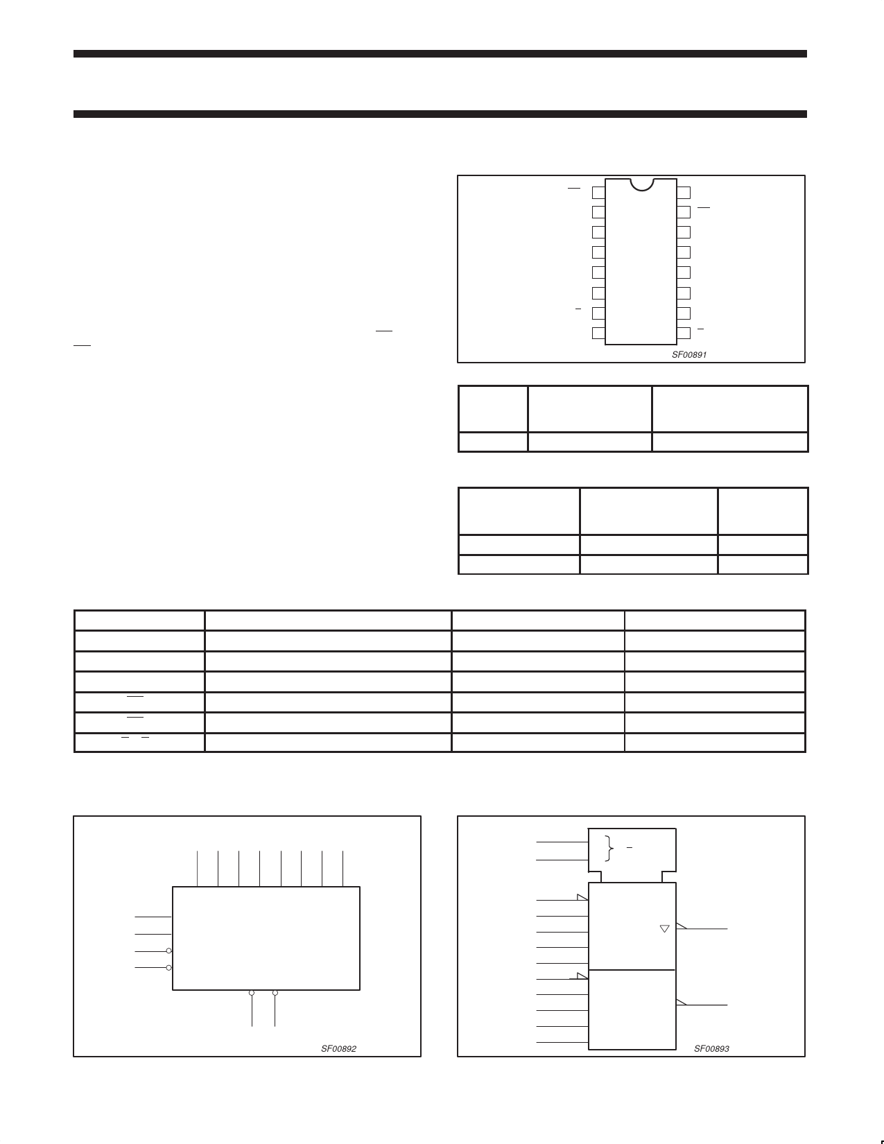
PIN CONFIGURATION
OEa 1
S1 2
I3a 3
I2a 4
I1a 5
I0a 6
Ya 7
GND 8
16 VCC
15 OEb
14 S0
13 I3b
12 I2b
11 I1b
10 I0b
9 Yb
SF00891
TYPE
74F353
TYPICAL
PROPAGATION
DELAY
6.0ns
TYPICAL
SUPPLY CURRENT
(TOTAL)
11mA
ORDERING INFORMATION
DESCRIPTION
16-pin plastic DIP
COMMERCIAL RANGE
VCC = 5V ±10%,
Tamb = 0°C to +70°C
N74F353N
16-pin plastic SO
N74F353D
PACKAGE
DRAWING
NUMBER
SOT38-4
SOT162-1
INPUT AND OUTPUT LOADING AND FAN-OUT TABLE
PINS
DESCRIPTION
74F (U.L.) HIGH/LOW
I0a–I3a
Port A data inputs
1.0/1.0
I0b–I3b
Port B data inputs
1.0/1.0
S0, S1
Common Select inputs
1.0/1.0
OEa
Port A Output Enable input (active Low)
1.0/1.0
OEb
Port B Output Enable input (active Low)
1.0/1.0
Ya, Yb
3-State outputs
150/40
NOTE:
One (1.0) FAST unit load is defined as: 20µA in the High state and 0.6mA in the Low state.
LOGIC SYMBOL
IEC/IEEE SYMBOL
LOAD VALUE HIGH/LOW
20µA/0.6mA
20µA/0.6mA
20µA/0.6mA
20µA/0.6mA
20µA/0.6mA
3mA/24mA
6 5 4 3 10 11 12 13
14
0 G0
2
1
3
I0a I1a I2a I3a I0b I1b I2b I3b
14
S0
2
S1
1
OEa
15
OEb
Ya Yb
VCC = Pin 16
GND = Pin 8
79
SF00892
1
MUX
EN
6
0
5
1
4
2
3
3
15
10
11
12
13
7
9
SF00893
1996 Jan 05
2
853–0103 16188
Share Link: 