74AHC595 데이터 시트보기 (PDF) - Diodes Incorporated.
부품명
상세내역
일치하는 목록
74AHC595 Datasheet PDF : 10 Pages
| |||
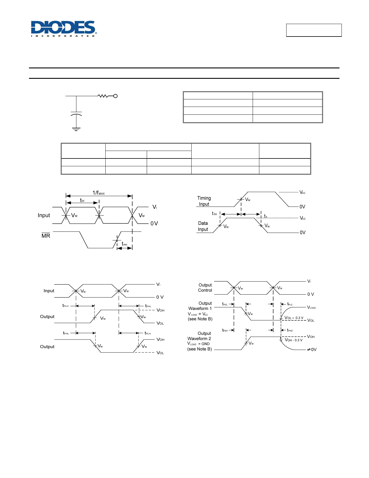
Parameter Measurement Information
From Output
Under Test
CL
(see Note A)
RL
VLOAD
Vcc
3.3V -3.6V
4.5V to 5.5V
Inputs
VI
tr/tf
VCC
3ns
VCC
3ns
TEST
tPLH/tPHL
tPLZ/tPZL
tPHZ/tPZH
VM
VCC/2
VCC/2
74AHC595
Vload
Open
VCC
GND
CL
15pF, 50pF
15pF, 50pF
Voltage Waveform
Pulse Duration and Recovery Time
Voltage Waveform
Set-up and Hold Times
Voltage Waveform
Propagation Delay Times
Inverting and Non Inverting Outputs
Voltage Waveform
Enable and Disable Times
Notes:
A .Includes test lead and test apparatus capacitance.
B. Output Waveform 1 depends on the internal QN node being low and behaves in this manner based on OE pin.
Output Waveform 2 depends on the internal QN node being high and behaves in this manner based on OE pin.
C. All pulses are supplied at pulse repetition rate ≤ 10 MHz
D. Inputs are measured separately one transition per measurement
E. tPLH and tPHL are the same as tPD.
74AHC595
Document number: DS35486 Rev. 3 - 2
Figure 2. Load Circuit and Voltage Waveforms
6 of 10
www.diodes.com
June 2013
© Diodes Incorporated
Share Link: 