74AHC1G09 데이터 시트보기 (PDF) - NXP Semiconductors.
부품명
상세내역
일치하는 목록
74AHC1G09 Datasheet PDF : 10 Pages
| |||
NXP Semiconductors
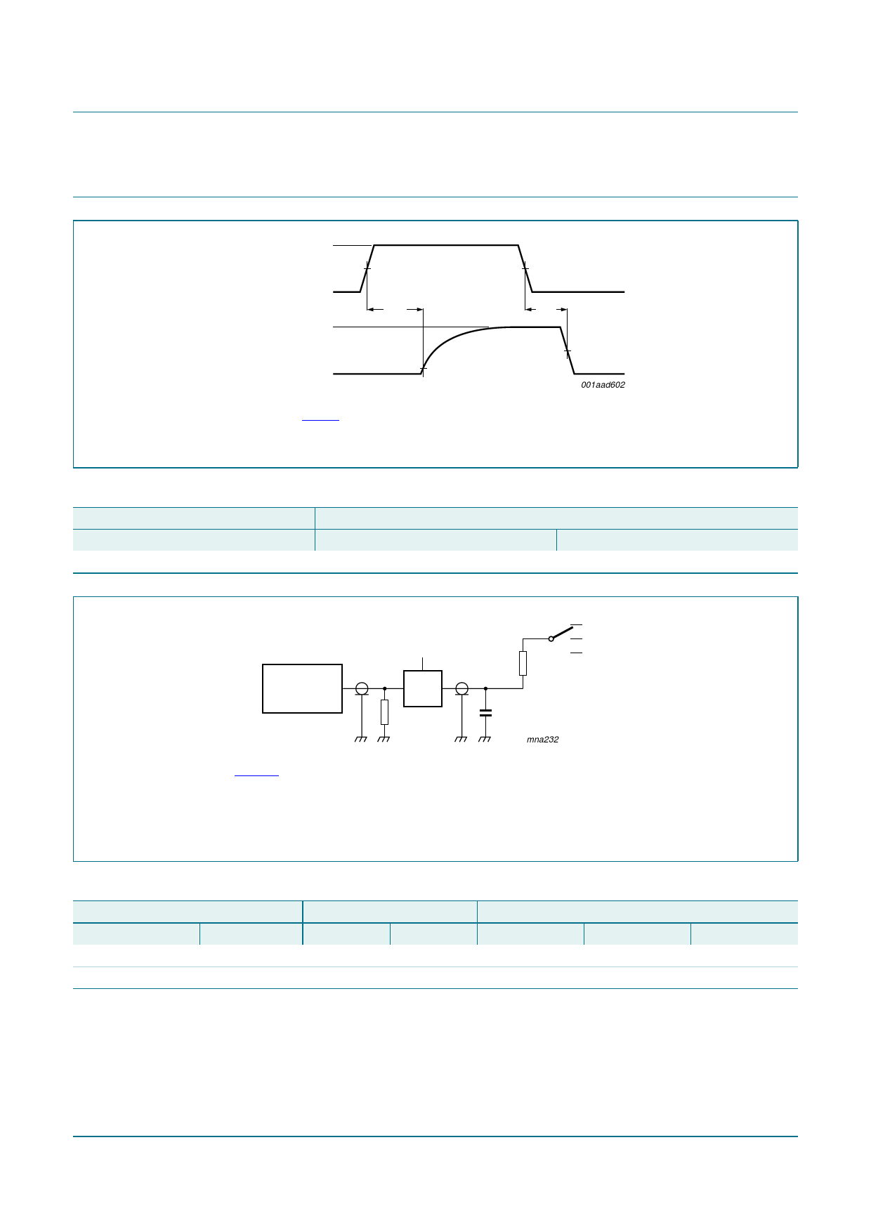
12. Waveforms
74AHC1G09
2-input AND gate with open-drain output
VI
A, B input
GND
Y output
VCC
VOL
VM
t PLZ
VX
Measurement points are given in Table 9.
VOL is the typical voltage output level that occur with the output load.
Fig 5. The data input (A, B) to output (Y) propagation delays
Table 9.
Input
VM
0.5VCC
Measurement points
Output
VM
0.5VCC
t PZL
VM
001aad602
VX
VOL + 0.3 V
VI
PULSE
GENERATOR
VCC
VO
D.U.T.
RT
S1
RL =
1000 Ω
CL
mna232
VCC
open
GND
Test data is given in Table 10.
Definitions for test circuit:
CL = Load capacitance including jig and probe capacitance.
RT = Termination resistance should be equal to output impedance Zo of the pulse generator.
Fig 6. Load circuit for switching times
Table 10. Test data
Input
VI
GND to VCC
GND to VCC
tr, tf
≤ 3.0 ns
≤ 3.0 ns
Load
RL
1000 Ω
1000 Ω
CL
15 pF
50 pF
S1
tPHZ, tPZH
GND
GND
tPLZ, tPZL
VCC
VCC
tPLH, tPHL
open
open
74AHC1G09_2
Product data sheet
Rev. 02 — 18 December 2007
© NXP B.V. 2007. All rights reserved.
5 of 10
Share Link: 