4051 데이터 시트보기 (PDF) - Unisonic Technologies
부품명
상세내역
일치하는 목록
4051 Datasheet PDF : 6 Pages
| |||
4051
CMOS IC
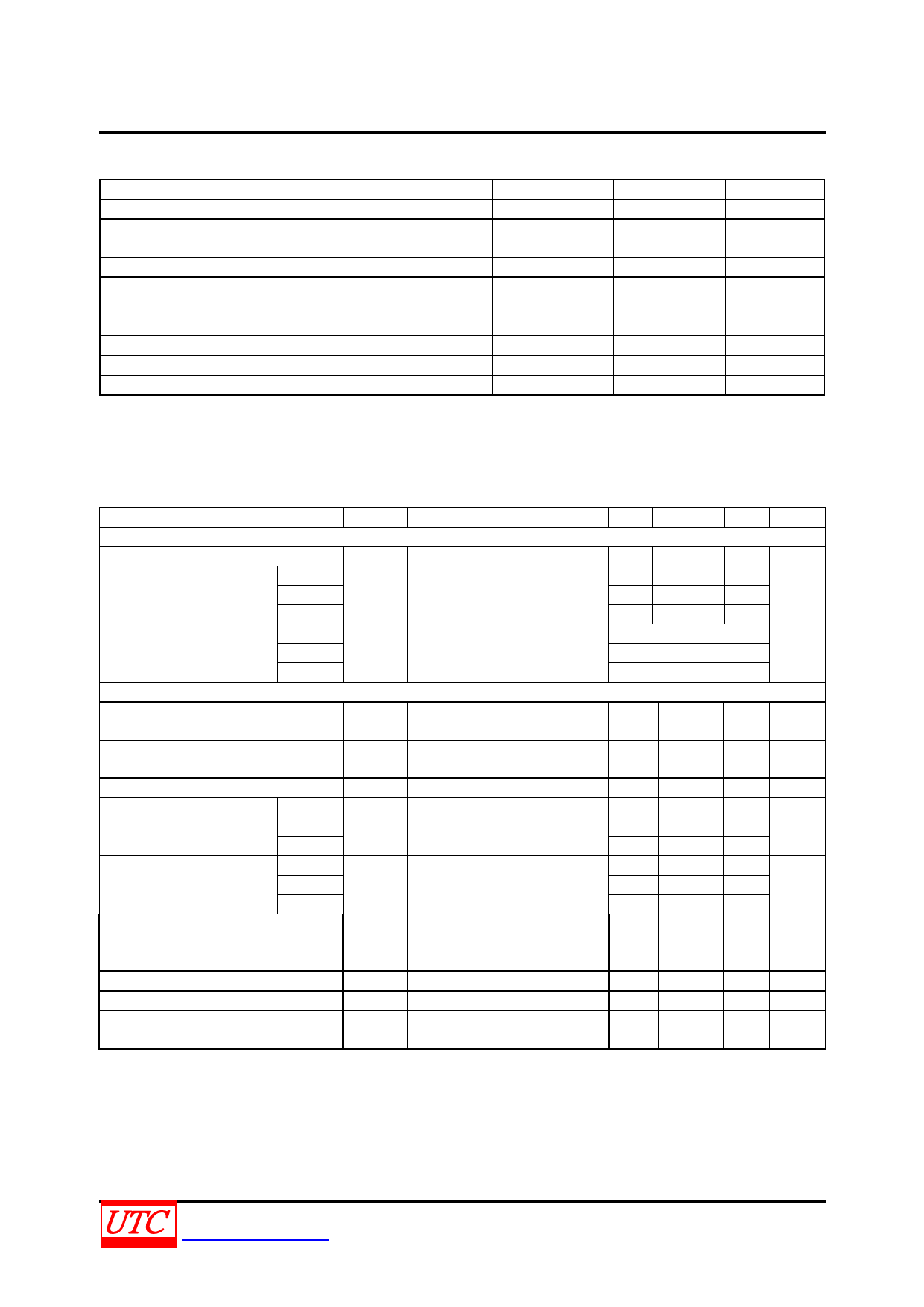
ABSOLUTE MAXIMUM RATING
PARAMETER
SYMBOL
RATINGS
UNIT
DC Supply Voltage (Referenced to VEE, VSS≧VEE)
VDD
-0.5 ~ +18
V
Input or Output Voltage (DC or Transient)
(Referenced to VSS for Control Inputs and VEE for Switch I/O)
VIN, VOUT
-0.5 ~ VDD +0.5
V
Input Current (DC or Transient), per Control Pin
IIN
±10
mA
Switch Through Current
ISW
±25
mA
Power Dissipation
Derating above 65℃
500
mW
PD
7
mW/℃
Junction Temperature
Operating Temperature Range
Storage Temperature Range
TJ
TOPR
TSTG
125
℃
-40 ~ +125
℃
-40 ~ +150
℃
Note: 1.Absolute maximum ratings are those values beyond which the device could be permanently damaged.
Absolute maximum ratings are stress ratings only and functional device operation is not implied.
2.The device is guaranteed to meet performance specification within 0℃~70℃ operating temperature range
and assured by design from –40℃~125℃.
ELECTRICAL CHARACTERISTICS (Ta=25℃, unless otherwise specified.)
PARAMETER
SYMBOL
TEST CONDITIONS
MIN TYP MAX
SUPPLY REQUIREMENTS (Voltages Referenced to VEE)
Power Supply Voltage Range
VDD VDD – 3.0≧VSS≧VEE
3
18
Quiescent Current per
Package
Total Supply Current
VDD=5V
VDD=10V
VDD=15V
VDD=5V
Control Inputs: VIN = VSS or VDD
IQ Switch I/O: VEE ≦VI/O ≦VDD,
and ∆Vsw≦500mV(Note 2)
0.005
5
0.010 10
0.015 20
Ta=25℃ only (The channel (0.07 µA/kHz) f + IQ
(Dynamic Plus Quiescent, VDD=10V ID(AV) component, (VIN-Vout)/Ron, is (0.20 µA/kHz) f + IQ
Per Package)
VDD=15V
not included.)
(0.36 µA/kHz) f + IQ
SWITCHES IN/OUT AND COMMONS OUT/IN -- X, Y, Z (Voltages Referenced to VEE)
Recommended Peak–to–Peak
Voltage Into or Out of the Switch
VI/O Channel On or Off
0
VDD
Recommended Static or Dynamic
Voltage Across the Switch
∆Vsw Channel On
0
600
Output Offset Voltage
ON Resistance
ΔON Resistance Between
Any Two Channels in the
Same Package
VDD=5V
VDD=10V
VDD=15V
VDD=5V
VDD=10V
VDD=15V
VO(OFF)
RON
VIN = 0V, No Load
∆Vsw≦500mV
VIN = VIL or VIH (Control), and
VIN = 0 to VDD (Switch)
∆RON
10
250 1050
120 500
80
280
25
70
10
50
10
45
Off–Channel Leakage Current
VIN = VIL or VIH (Control)
IOFF Channel to Channel or Any
One Channel, VDD=15V
±0.05 ±100
Capacitance, Switch I/O
CI/O Inhibit = VDD
10
Capacitance, Common O/I
CO/I Inhibit = VDD
17
Capacitance, Feedthrough
Pins Not Adjacent
0.15
(Channel Off)
CI/O Pins Adjacent
0.47
UNIT
V
µA
µA
VPP
mV
µV
Ω
Ω
nA
pF
pF
pF
UNISONIC TECHNOLOGIES CO., LTD
www.unisonic.com.tw
3 of 6
QW-R502-054,A
Share Link: 