PI2BV3877L 데이터 시트보기 (PDF) - Pericom Semiconductor
부품명
상세내역
일치하는 목록
PI2BV3877L Datasheet PDF : 4 Pages
| |||
PI2BV3877 111222333444555666777888999000111222333444555666777888999000111222333444555666777888999000111222111222333444555666777888999000111222333444555666777888999000111222333444555666777888999000111222111222333444555666777888999000111222333444555666777888999000111222333444555666777888999000111222111222333444555666777888999000111222333444555666777888999000111222333444555666777888999000111222111222333444555666777888999000111222
2.5V, 10-Bit, 2-Port
266 MHz DDR Bus Switch
Product Features
• Used in X4 DDR modules
• Near zero propagation delay
• 20-ohm switches connect inputs to outputs
• Fast Switching Speed –3ns (max.)
• Low Off Capacitance (3pF)
• Pull-down on B output
• Packages available:
– 24-pin 150 mil wide plastic QSOP (Q)
– 24-pin 173 mil wide plastic TSSOP (L)
Product Description
Pericom Semiconductor’s PI2B series of logic circuits are produced
using the Company’s advanced submicron CMOS technology,
achieving industry leading performance.
The PI2BV3877 is a 10-bit, 2.5 volt two-port bus switch designed with
a low ON resistance allowing inputs to be connected directly to
outputs. The bus switch creates no additional propagational delay
or additional ground bounce noise. The switches are turned ON by
the Bus Enable (BEN) input signals.
The PI2BV3877 switch is intended for 266 MHz DDR (X4) Memory
Module Applications.
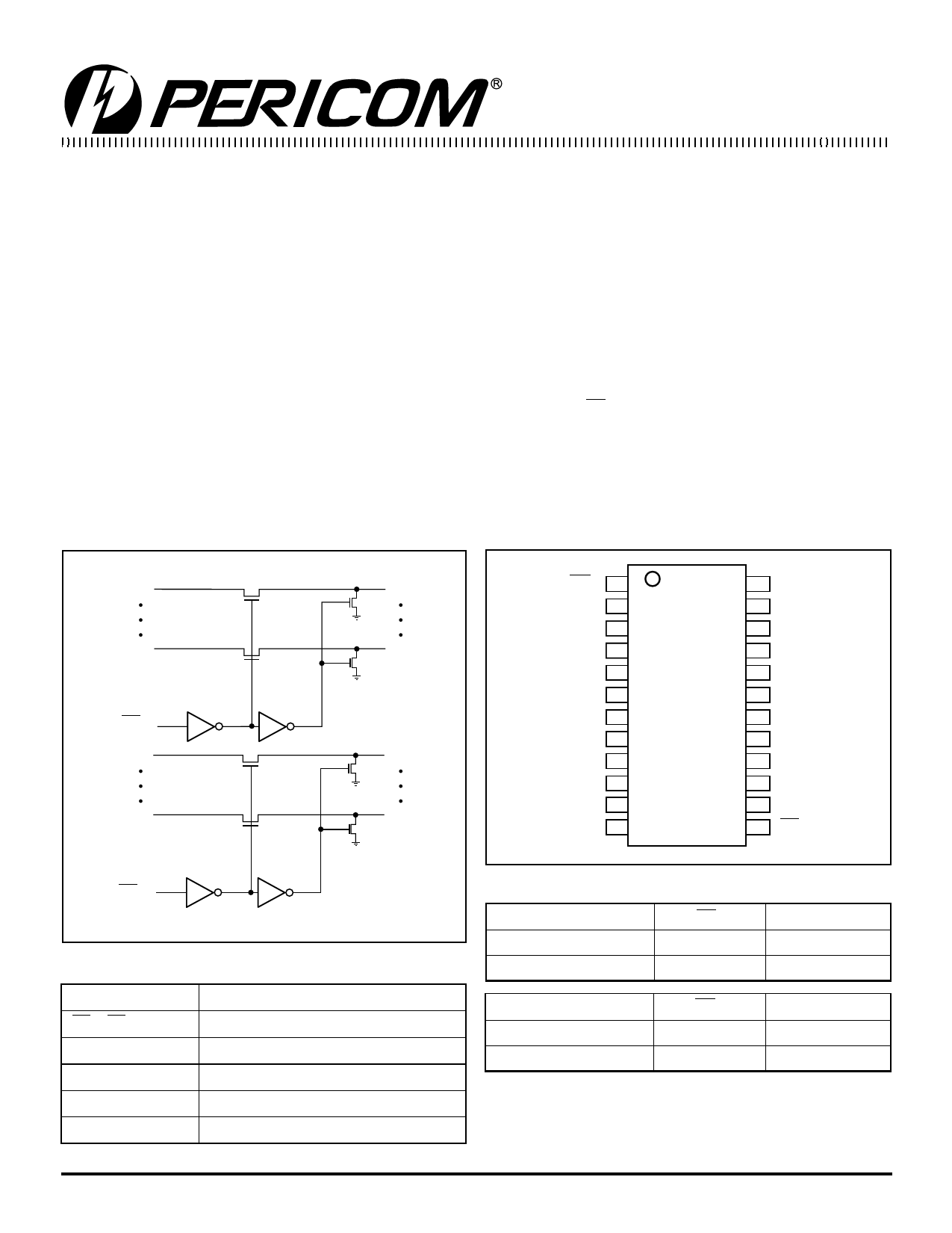
Logic Block Diagram
A0
B0
A4
B4
BE0
A5
B5
A9
B9
BE1
Product Pin Description
Pin Name
Description
BE0, BE1
Bus Enable Input (Active Low)
A0–4, A5-9
Bus A
B0-4, B5-9
Bus B
GND
Ground
VCC
Power
Product Pin Configuration
BE0
A0
A1
A2
A3
A4
A5
A6
A7
A8
A9
GND
1
24
2
23
3
22
4
21
5 24-Pin 20
6 Q, L 19
7
18
8
17
9
16
10
15
11
14
12
13
VCC
B0
B1
B2
B3
B4
B5
B6
B7
B8
B9
BE1
Truth Table(1)
Function
BE0
Disconnect
H
Connect
L
Function
BE1
Disconnect
H
Connect
L
Notes:
1. H = High Voltage Level
L = Low Voltage Level
Hi-Z = High Impedance
1
A0 – A4
Hi-Z
B0-4
A5 – A9
Hi-Z
B5-B9
PS8472D 11/14/01
Share Link: 