MC74VHC1G01 데이터 시트보기 (PDF) - ON Semiconductor
부품명
상세내역
일치하는 목록
MC74VHC1G01 Datasheet PDF : 6 Pages
| |||
MC74VHC1G01
Single 2−Input NAND Gate
with Open Drain Output
The MC74VHC1G01 is an advanced high speed CMOS 2−input
NAND gate with an open drain output fabricated with silicon gate
CMOS technology.
The internal circuit is composed of multiple stages, including an
open drain output which provides the ability to set output switching
level. This allows the MC74VHC1G01 to be used to interface 5.0 V
circuits to circuits of any voltage between VCC and 7.0 V using an
external resistor and power supply.
The MC74VHC1G01 input structure provides protection when
voltages up to 7.0 V are applied, regardless of the supply voltage.
Features
• High Speed: tPD = 3.7 ns (Typ) at VCC = 5.0 V
• Low Internal Power Dissipation: ICC = 1 mA (Max) at TA = 25°C
• Power Down Protection Provided on Inputs
• Pin and Function Compatible with Other Standard Logic Families
• Chip Complexity: FETs = 62
• Pb−Free Packages are Available
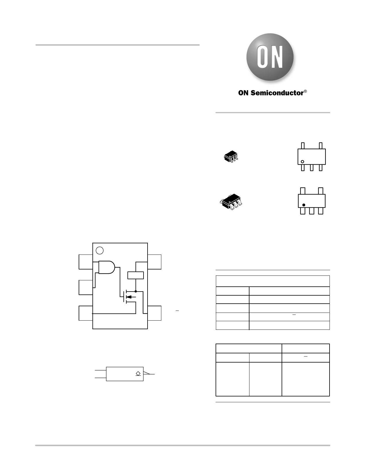
IN B 1
IN A 2
OVT
5 VCC
GND 3
4 OUT Y
Figure 1. Pinout (Top View)
IN A
&
IN B
Figure 2. Logic Symbol
OUT Y
http://onsemi.com
MARKING
DIAGRAMS
SC−88A / SOT−353 / SC−70
DF SUFFIX
CASE 419A
V0 M G
G
TSOP−5 / SOT−23 / SC−59
DT SUFFIX
CASE 483
V0AYW
G
M
= Date Code
A
= Assembly Location
Y
= Year
W
= Work Week
G
= Pb−Free Package
(Note: Microdot may be in either location)
PIN ASSIGNMENT
1
IN B
2
IN A
3
GND
4
OUT Y
5
VCC
FUNCTION TABLE
Inputs
A
B
L
L
L
H
H
L
H
H
Output
Y
Z
Z
Z
L
ORDERING INFORMATION
See detailed ordering and shipping information in the package
dimensions section on page 4 of this data sheet.
© Semiconductor Components Industries, LLC, 2005
1
June, 2005 − Rev. 14
Publication Order Number:
MC74VHC1G01/D
Share Link: 