74HC595BQ-Q100(2017) 데이터 시트보기 (PDF) - NXP Semiconductors.
부품명
상세내역
일치하는 목록
74HC595BQ-Q100
(Rev.:2017)
(Rev.:2017)
NXP Semiconductors.

74HC595BQ-Q100 Datasheet PDF : 23 Pages
| |||
Nexperia
74HC595-Q100; 74HCT595-Q100
8-bit serial-in, serial or parallel-out shift register with output latches; 3-state
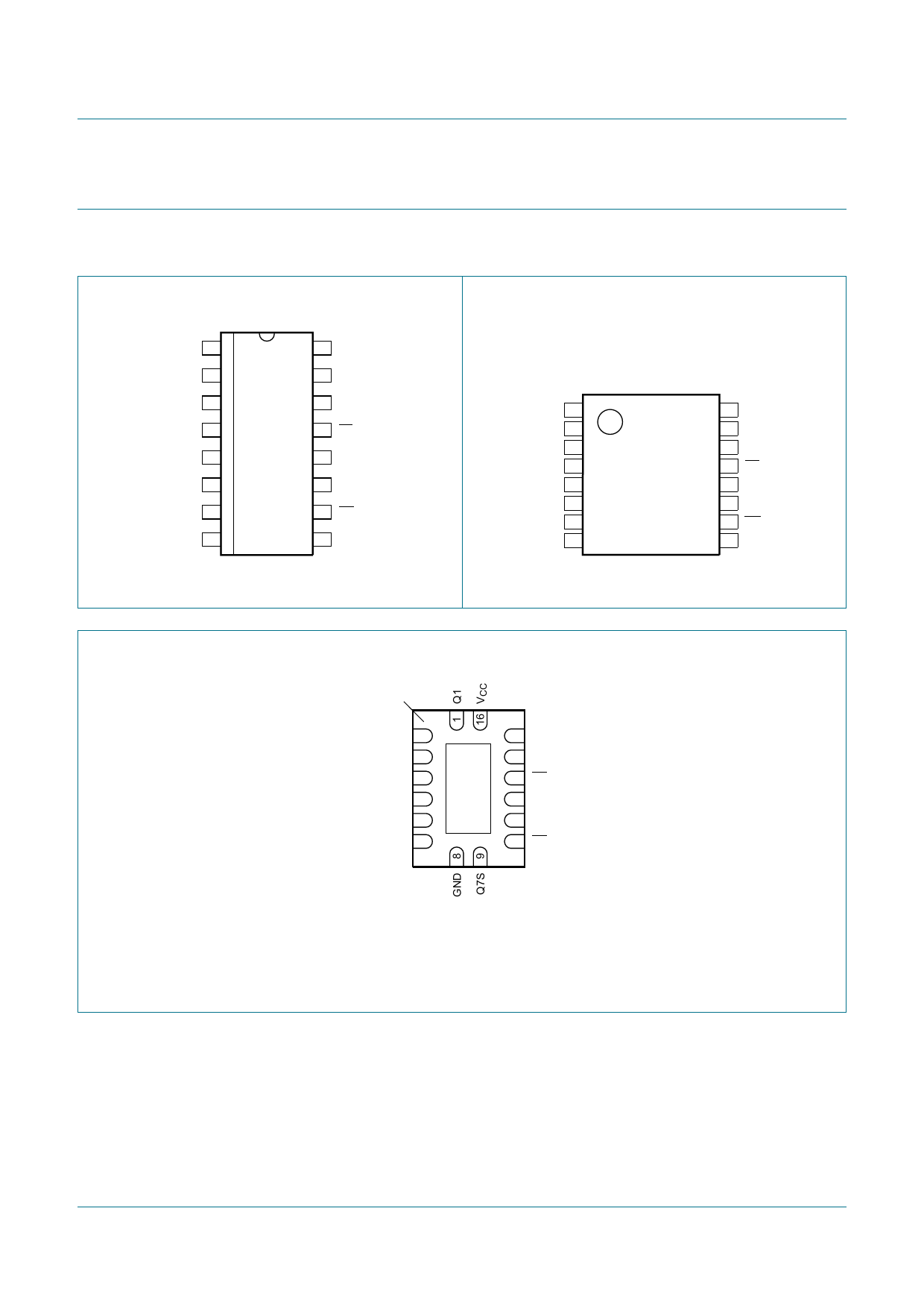
6 Pinning information
6.1 Pinning
74HC595-Q100
74HCT595-Q100
Q1 1
Q2 2
16 VCC
15 Q0
Q3 3
14 DS
Q4 4
13 OE
Q5 5
12 STCP
Q6 6
11 SHCP
Q7 7
10 MR
GND 8
9 Q7S
aaa-003476
Figure 5. Pin configuration for SO16
74HC595-Q100
74HCT595-Q100
Q1 1
Q2 2
Q3 3
Q4 4
Q5 5
Q6 6
Q7 7
GND 8
16 VCC
15 Q0
14 DS
13 OE
12 STCP
11 SHCP
10 MR
9 Q7S
aaa-003477
Figure 6. Pin configuration for (T)SSOP16
terminal 1
index area
74HC595-Q100
74HCT595-Q100
Q2 2
Q3 3
Q4 4
Q5 5
Q6 6
Q7 7
GND(1)
15 Q0
14 DS
13 OE
12 STCP
11 SHCP
10 MR
aaa-003478
Transparent top view
(1) This is not a supply pin. The substrate is attached to this pad using conductive die attach material. There is no
electrical or mechanical requirement to solder this pad. However, if it is soldered, the solder land should remain floating or
be connected to GND.
Figure 7. Pin configuration for DHVQFN16
74HC_HCT595_Q100
Product data sheet
All information provided in this document is subject to legal disclaimers.
Rev. 3 — 28 February 2017
© Nexperia B.V. 2017. All rights reserved.
4 / 23
Share Link: