STV8130A 데이터 시트보기 (PDF) - STMicroelectronics
부품명
상세내역
일치하는 목록
STV8130A
STMicroelectronics

STV8130A Datasheet PDF : 12 Pages
| |||
CIRCUIT DESCRIPTION
3 CIRCUIT DESCRIPTION
STV8130AD
The STV8130A# and STV8130D# are dual-voltage regulators with Reset and Disable functions.
The two regulation parts are supplied from a single voltage reference circuit trimmed by zener
zapping during EWS testing. Since the supply voltage of this voltage reference is connected to pin
INPUT1 (VIN1), the second regulator will not work if pin INPUT1 is not supplied.
The adjustable voltage of pin OUTPUT2 (VOUT2) is defined by output bridge resistors (R1, R2): the
values of these resistors are calculated to obtain, with the targetted value for VOUT2, the reference
voltage (VREF = 2.44 V) on the median point connected to pin PROGRAM.
The output stages are designed using a Darlington configuration with a typical dropout voltage of
1.2 V.
The Disable circuit will switch off pin OUTPUT2 if a voltage less than 0.8 V is applied to pin
DISABLE.
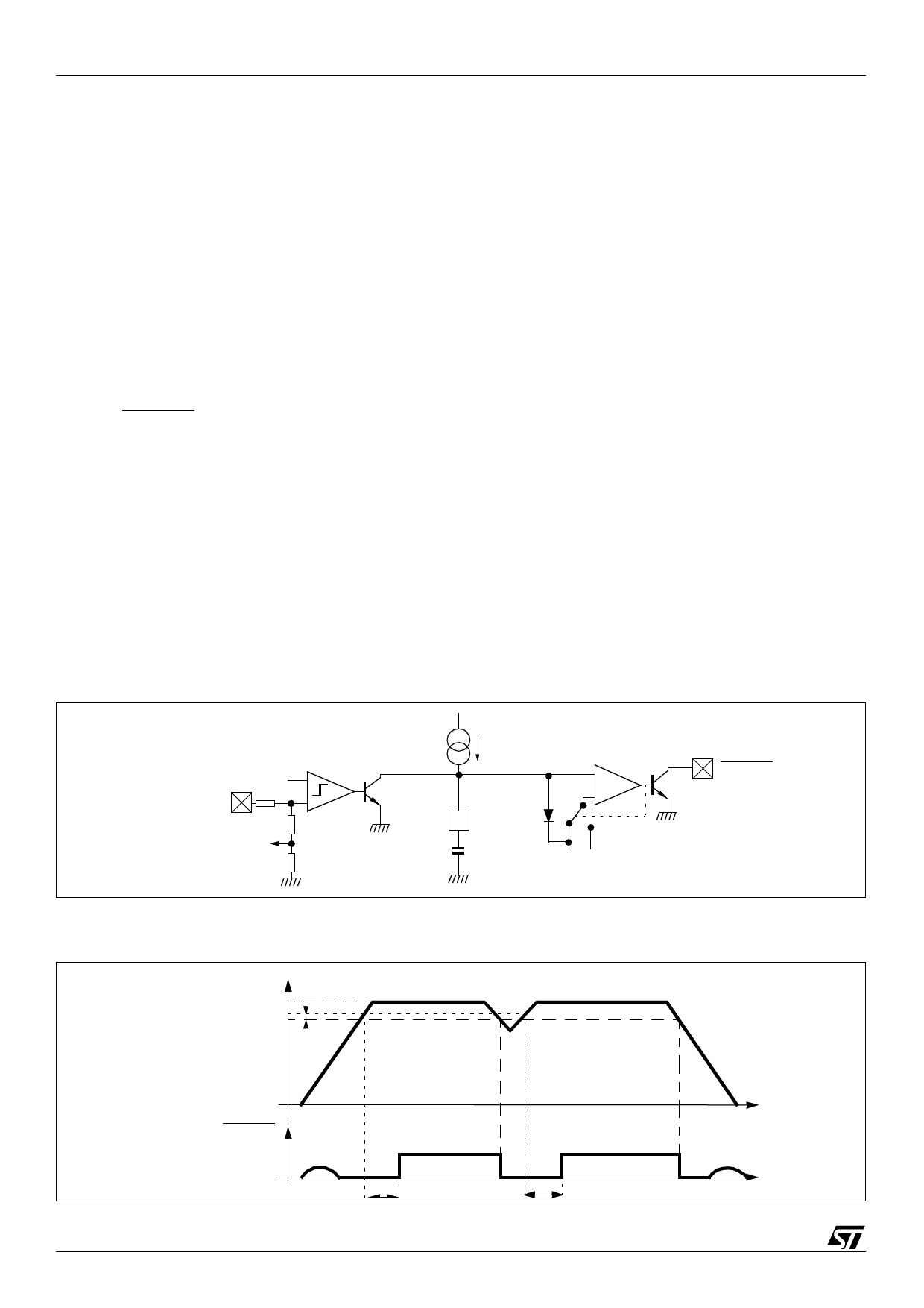
The Reset circuit checks the voltage at pin OUTPUT1. If this voltage drops below VOUT1 - 0.25 V
(3.05 V Typ.), the "a" comparator (Figure 3) rapidly discharges the external capacitor (Ce) and the
reset output immediately switches to low. This drop can be caused by a parasitic loading condition
on pin OUTPUT1 or by a too low value of VIN (short powering off). When the voltage at pin
OUTPUT1 exceeds VOUT1 - 0.2 V (3.1 V Typ.), the VCe voltage increases linearly to the reference
voltage (VREF = 2.44 V) corresponding to a Reset Pulse Delay (tRD) as shown in Figure 4.
tRD = C-----e---1-×--0---2-µ--.--A4---4----V--
Afterwards, the reset output returns to high. To avoid glitches in the reset output, the second
comparator "b" has a large hysteresis (1.84 V).
Figure 3: Reset Diagram
OUTPUT1
VREF
+a
- 50
REG
VREF = 2.44 V
10 µA
3
Ce
-b
+
VREF 0.6V
RESET
Figure 4: Internal Reset Voltages
VOUT1
K
VO1RST
VRTH
RESET
K = Actual Value of VOUT1
Power On tRD
tRD
6/12
Power Off
Share Link: