S1M8662A 데이터 시트보기 (PDF) - Samsung
부품명
상세내역
일치하는 목록
S1M8662A Datasheet PDF : 22 Pages
| |||
RX IF/BBA WITH GPS
S1M8662A (Preliminary)
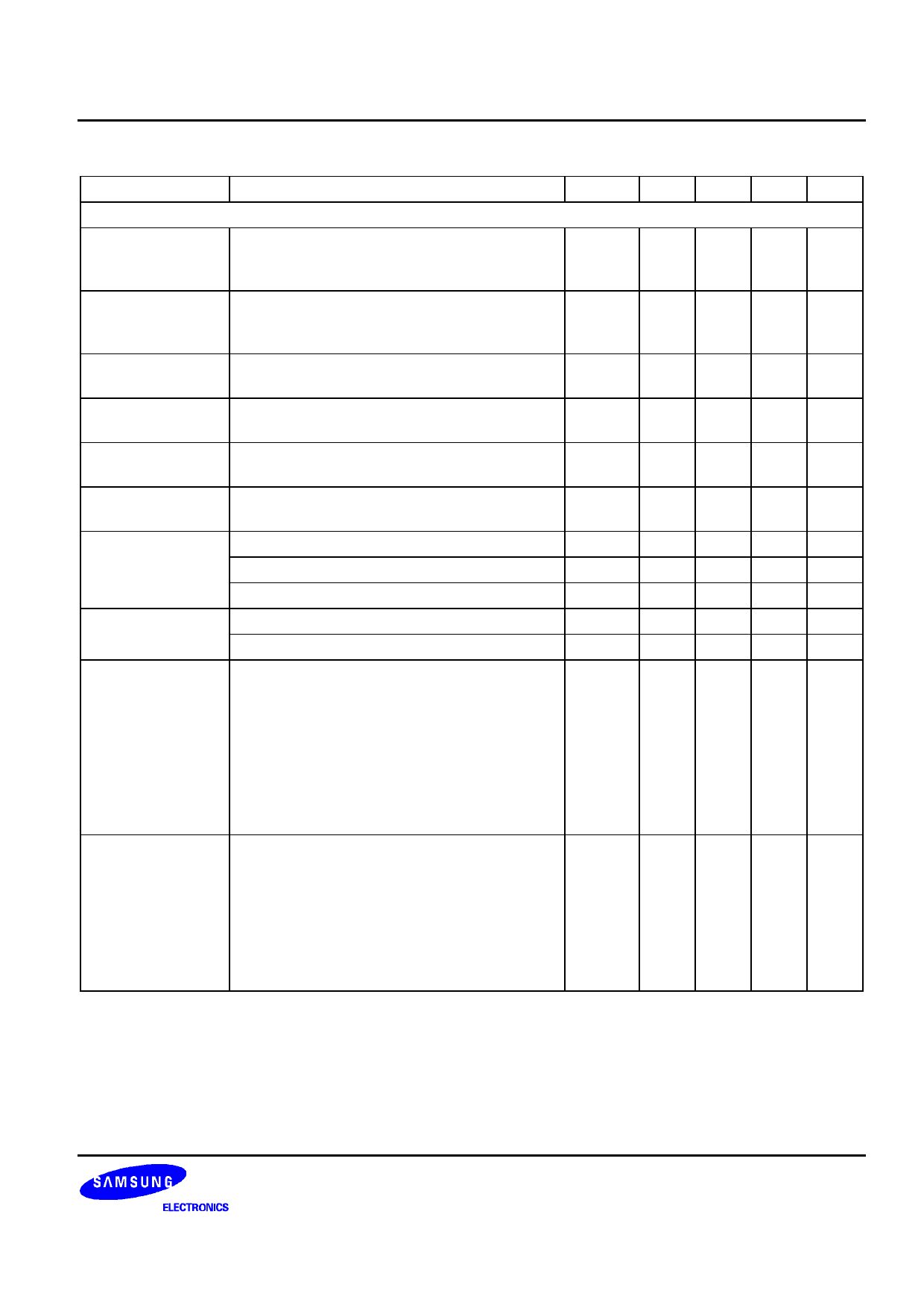
AC Characteristics
Characteristic
Test Conditions
Symbol Min Typ Max Unit
CDMA Performance
Input sensitivity
Maximum AGC gain. Control input signal so VCSEN -102 -
that output corresponding to 3LSB is output
from ADC.
- dBm
Maximum input
signal
Minimum AGC gain. Control input signal so VCMAX -
that output corresponding to 3LSB is output
from ADC.
-
-12 dBm
AGC gain slope PDM 3.3V Mode
GS
43 50 57 dB/V
LOPE
AGC gain error
-30 to +85°C.
over temperature
GVAR -3
-
3
dB
IF input frequency Cin < 2pF
range
Fin
-
-
250 MHz
IF input
Impedance
Zin
0.8 1.0 1.2 kΩ
Input power = -102dBm
NFmin -
-
7
dB
Noise figure
Input power = -75dBm
NFmid -
-
20 dB
Input power = -25dBm
NFmax -
-
72 dB
IIP3
AGC gain Max.
IIP3max -53
-
- dBm
AGC gain Min.
IIP3min -10
-
- dBm
Spurious contents ADC generated harmonic frequency
TSpur
-
component. Two signals in the in-band are
each mixed with signals which will allow ADC
to produce -7dB output signals. The harmonic
and non-harmonic components of the ADC
output signals between 1kHz to 20MHz are
extracted and added. The AGC control
voltage is controlled so that ADC output is full
scale when the input signal is -80dBm.
-
-25 dBc
Spurious content In-band spurious peak value produced by IMD Jspur
-
related to jammer based on 2 jammer signals.
One in-band signal(@50kHz,0.5*F/S)
and two jammers(@900kHz, 22dB*F/S and
@1.7MHz, 21dB*F/S)are simultaneously
input. AGC control voltage is controlled so
that ADC output is F/S when the input signal
is -80dBm.
- -18.4 dBc
7
Share Link: 