IP137MLCC4 데이터 시트보기 (PDF) - Semelab - > TT Electronics plc
부품명
상세내역
일치하는 목록
IP137MLCC4 Datasheet PDF : 2 Pages
| |||
IP137MAHVH
IP137MHVHA
LM137HVH
IP137MAH
IP137MH
LM137H
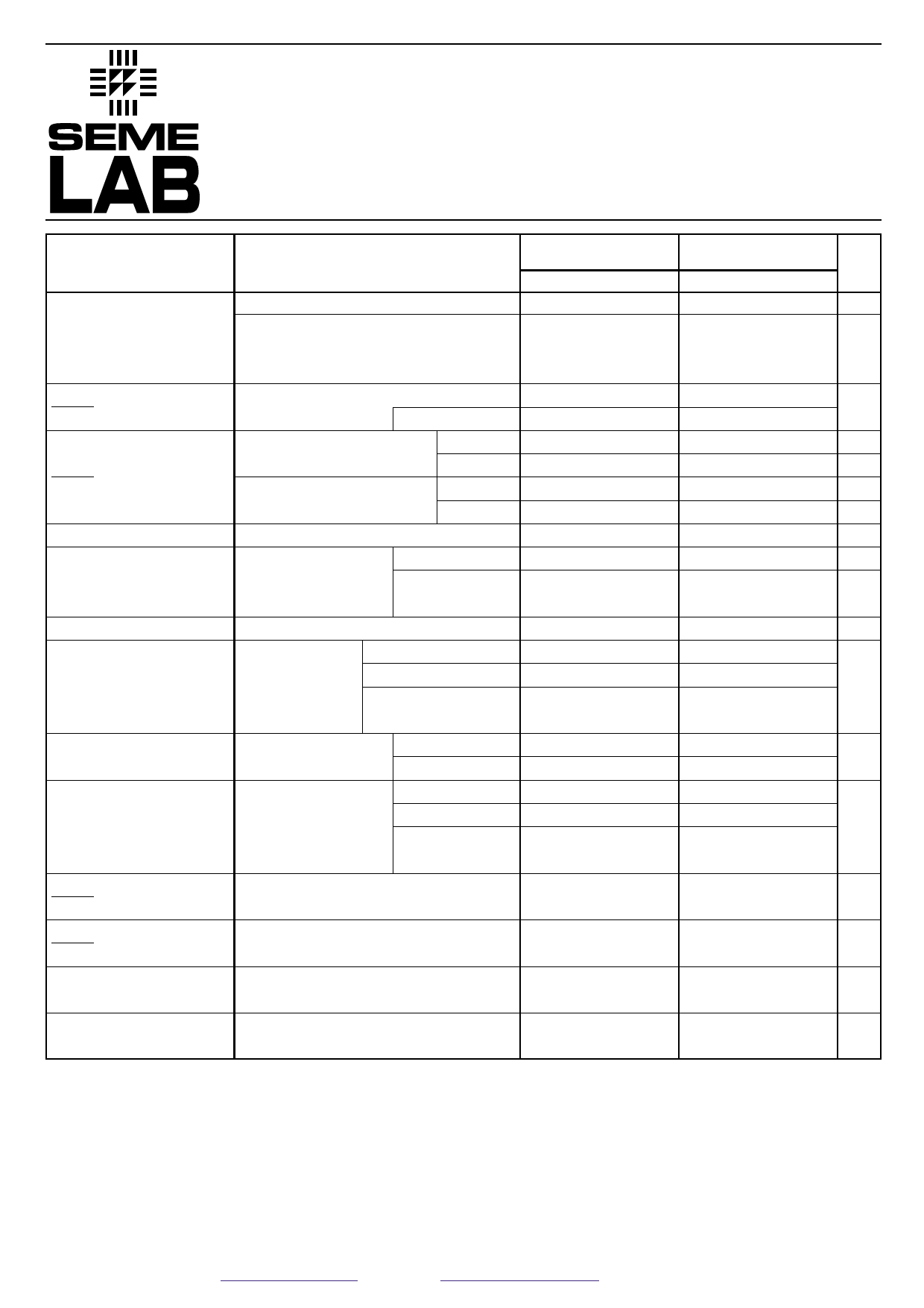
Parameter
VREF Reference Voltage
DVOUT
DVIN
Line Regulation 1
DVOUT
DIOUT
Load Regulation 1
Thermal Regulation
Ripple Rejection
IADJ Adjust Pin Current
DIADJ Adjust Pin Current
Change
IMIN Minimum Load
Current
ICL
Current Limit
DVOUT Temperature
DTEMP Stability
DVOUT
DTIME
Long Term Stability
en
RqJC
RMS Output Noise
(% of VOUT)
Thermal Resistance
Junction to Case
Test Conditions
IOUT = 10mA
IOUT = 10mA to IMAX
VIN – VOUT = 3V to VMAX
P £ PMAX
TJ = -55 to 150°C
VIN – VOUT = 3V to VMAX
IOUT = 10mA to IMAX
IOUT = 10mA to IMAX
TJ = -55 to 150°C
TJ = -55 to 150°C
VOUT £ 5V
VOUT ³ 5V
VOUT £ 5V
VOUT ³ 5V
tp = 10ms
TA = 25°C
VOUT = -10V
f = 120Hz
CADJ = 0
CADJ = 10mF
TJ = -55 to 150°C
TJ = -55 to 150°C
IOUT = 10mA to IMAX
TJ = -55 to +150°C
VIN – VOUT = 3V to 40V
VIN – VOUT = 3V to 50V
(HV SERIES)
TJ = -55 to 150°C
VIN – VOUT £ 40V
VIN – VOUT £ 10V
VIN – VOUT £ 15V
TJ = -55 to 150°C
VIN – VOUT = 40V
VIN – VOUT = 50V
(HV SERIES)
TJ = -55 to 150°C
TA = +125°C
t = 1000 Hrs
f = 10 Hz to 10 kHz
TA = 25°C
H Package
IP137MAHV
IP137MA
Min. Typ. Max.
-1.238 -1.25 -1.262
-1.220 -1.25 -1.280
0.005 0.010
0.010 0.030
5
25
0.1 0.5
10
50
0.2
1
0.002 0.020
60
66
70
80
65 100
0.2
2
1.0
5
2.0
6
2.5
5
1.2
3
0.50 0.80 1.5
0.15 0.17
0.10 0.17 0.5
0.6 1.5
0.3
1
0.003
12
15
IP137MHV , IP137M
LM137HV , LM137
Min. Typ. Max. Units
-1.225 -1.25 -1.275 V
-1.200 -1.25 -1.300 V
0.010
0.020
15
0.3
20
0.3
0.002
60
0.020
%/V
0.050
25 mV
0.5 %
50 mV
1
%
0.02 %/W
dB
66
77
dB
65 100 mA
0.5
5
2
5
mA
3
6
2.5
5
mA
1.2
3
0.50 0.80 1.5
0.15 0.17
A
0.10 0.17 0.5
0.6
%
0.3
1
%
0.003
%
12
15 °C/W
1) Regulation is measured at constant junction temperature, using pulse testing at a low duty cycle. Changes in output voltage due to
heating effects are covered under thermal regulation specifications. Load regulation is measured at a point 1/8” from the bottom of
the package for the TO–3 and TO–66 packages, at the junction of the wide and narrow portion of the output lead for the
SMD1package, and 1/8” below the base of the package on the output pin of the TO–257 package.
2) Test Conditions unless otherwise stated: VIN – VOUT = 5V , IOUT = 0.1A , PMAX = 2W , IMAX = 0.5A
VMAX = 40V for standard series , 50V for HV series.
Semelab plc. Telephone +44(0)1455 556565. Fax +44(0)1455 552612.
E-mail: sales@semelab.co.uk Website: http://www.semelab.co.uk
Prelim. 7/00
Share Link: 