NJU6682 데이터 시트보기 (PDF) - Japan Radio Corporation
부품명
상세내역
일치하는 목록
NJU6682 Datasheet PDF : 58 Pages
| |||
NJU6682
(3)Explanation of Instruction Code
3-1)Display ON/OFF
This instruction executes whole display ON/OFF without relationship of the data in the Display Data RAM and internal
conditions.
(R/W)
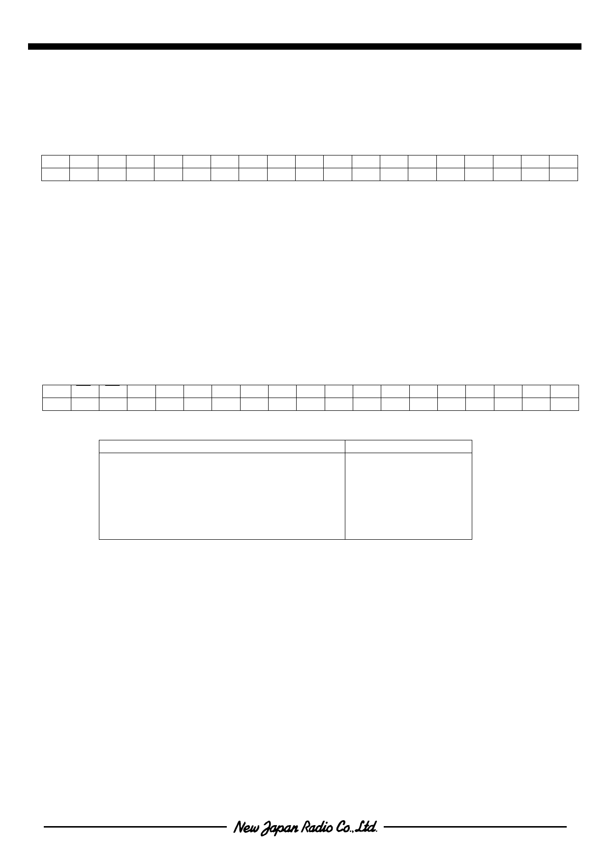
A0 RD WR D15 D14 D13 D12 D11 D10 D9 D8 D7 D6 D5 D4 D3 D2 D1 D0
01000000000* * * * * * *D
* : Don’t Care
D=0:Display OFF
D=1:Display ON
3-2)Z Address Set
This instruction sets the line address of Display Data RAM which correspond to COM0 terminal (Normally, it means the
most upper line of the display ). The display area is only the number of lines which is equivalent to display duty in the
increasing direction from the line address is automatically.
At that time, the data of Display Data RAM isn’t changed at all. When the RAM mapping is set to Variable RAM
Mapping Mode, the status of Variable RAM Mapping takes priority over this instruction. Therefore, the status of this Z
Address Set instruction will be unavailable.
(R/W)
A0 RD WR D15 D14 D13 D12 D11 D10 D9 D8 D7 D6 D5 D4 D3 D2 D1 D0
0 1 0 0 0 1 0 1 0 1 A8 A7 A6 A5 A4 A3 A2 A1 A0
R/W
A8 A7 A6 A5 A4 A3 A2 A1 A0
000000000
000000001
:
:
:
100111110
100111111
Z Address (HEX)
0
1
:
:
:
13E
13F
Share Link: 