TK12A55D 데이터 시트보기 (PDF) - Toshiba
부품명
상세내역
일치하는 목록
TK12A55D Datasheet PDF : 6 Pages
| |||
TK12A55D
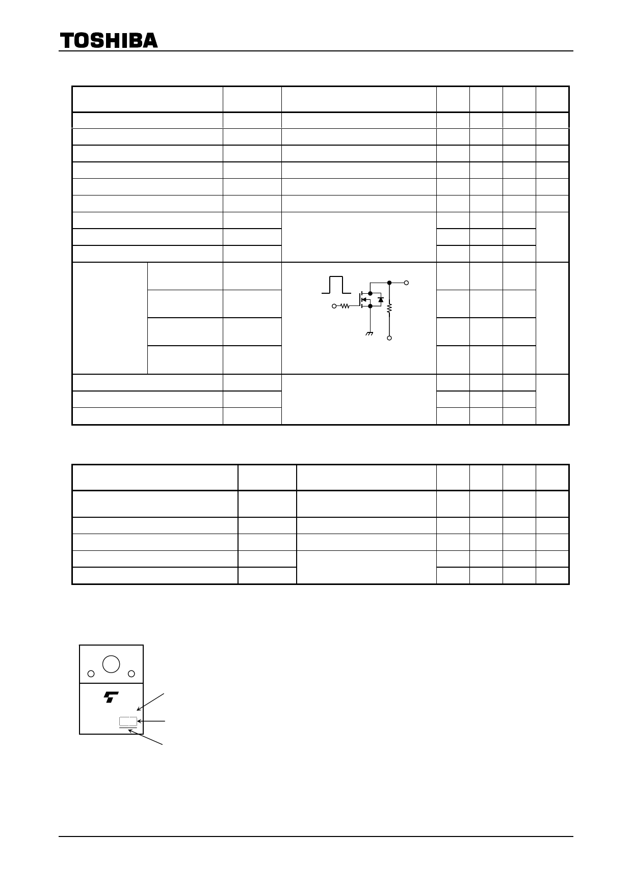
Electrical Characteristics (Ta = 25°C)
Characteristics
Gate leakage current
Drain cut-off current
Drain-source breakdown voltage
Gate threshold voltage
Drain-source ON resistance
Forward transfer admittance
Input capacitance
Reverse transfer capacitance
Output capacitance
Rise time
Switching time
Turn-on time
Fall time
Turn-off time
Total gate charge
Gate-source charge
Gate-drain charge
Symbol
Test Condition
Min Typ. Max Unit
IGSS
IDSS
V (BR) DSS
Vth
RDS (ON)
|Yfs|
Ciss
Crss
Coss
VGS = ±30 V, VDS = 0 V
VDS = 550 V, VGS = 0 V
ID = 10 mA, VGS = 0 V
VDS = 10 V, ID = 1 mA
VGS = 10 V, ID = 6 A
VDS = 10 V, ID = 6 A
VDS = 25 V, VGS = 0 V, f = 1 MHz
⎯
⎯
±1
μA
⎯
⎯
10
μA
550 ⎯
⎯
V
2.0
⎯
4.0
V
⎯ 0.48 0.57 Ω
1.5 6.0
⎯
S
⎯ 1550 ⎯
⎯
7
⎯
pF
⎯ 165 ⎯
tr
10 V
VGS
ID = 6 A VOUT
⎯
25
⎯
0V
ton
50 Ω
RL = 33 Ω ⎯
60
⎯
ns
tf
⎯
15
⎯
VDD ≈ 200 V
toff
Duty ≤ 1%, tw = 10 μs
⎯ 110 ⎯
Qg
⎯
28
⎯
Qgs
VDD ≈ 400 V, VGS = 10 V, ID = 12 A
⎯
18
⎯
nC
Qgd
⎯
10
⎯
Source-Drain Ratings and Characteristics (Ta = 25°C)
Characteristics
Continuous drain reverse current
(Note 1)
Pulse drain reverse current
(Note 1)
Forward voltage (diode)
Reverse recovery time
Reverse recovery charge
Symbol
IDR
IDRP
VDSF
trr
Qrr
Test Condition
⎯
⎯
IDR = 12 A, VGS = 0 V
IDR = 12 A, VGS = 0 V,
dIDR/dt = 100 A/μs
Min Typ. Max Unit
⎯
⎯
12
A
⎯
⎯
48
A
⎯
⎯
−1.7
V
⎯ 1300 ⎯
ns
⎯
13
⎯
μC
Marking
K12A55D
Note 4: A line under a Lot No. identifies the indication of product Labels
[[G]]/RoHS COMPATIBLE or [[G]]/RoHS [[Pb]]
Part No.
(or abbreviation code)
Lot No.
Note 4
Please contact your TOSHIBA sales representative for details as to
environmental matters such as the RoHS compatibility of Product.
The RoHS is Directive 2002/95/EC of the European Parliament and
of the Council of 27 January 2003 on the restriction of the use of certain
hazardous substances in electrical and electronic equipment.
2
2011-04-26
Share Link: 