K12X60U 데이터 시트보기 (PDF) - Toshiba
부품명
상세내역
일치하는 목록
K12X60U Datasheet PDF : 3 Pages
| |||
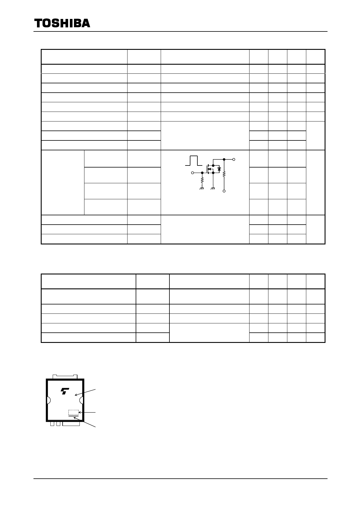
Electrical Characteristics (Ta = 25°C)
TK12X60U
Characteristics
Gate leakage current
Drain cut-off current
Drain-source breakdown voltage
Gate threshold voltage
Drain-source ON resistance
Forward transfer admittance
Input capacitance
Reverse transfer capacitance
Output capacitance
Rise time
Switching time
Turn-on time
Fall time
Turn-off time
Total gate charge
Gate-source charge
Gate-drain charge
Symbol
Test Condition
Min Typ. Max Unit
IGSS
VGS = ±30 V, VDS = 0 V
⎯
⎯
±1
µA
IDSS
VDS = 600 V, VGS = 0 V
⎯
⎯
100
µA
V (BR) DSS ID = 10 mA, VGS = 0 V
600 ⎯
⎯
V
Vth
VDS = 10 V, ID = 1 mA
3.0
⎯
5.0
V
RDS (ON) VGS = 10 V, ID = 6 A
⎯ 0.36 0.4
Ω
⎪Yfs⎪
VDS = 10 V, ID = 6 A
2.0 7.0
⎯
S
Ciss
⎯ 720 ⎯
Crss
VDS = 10 V, VGS = 0 V, f = 1 MHz
⎯
55
⎯
pF
Coss
⎯ 1700 ⎯
tr
10 V
VGS
ID = 6A VOUT
⎯
30
⎯
0V
ton
50 Ω
RL =
50Ω
⎯
60
⎯
ns
tf
VDD ∼− 300 V
⎯
8
⎯
toff
Duty <= 1%, tw = 10 µs
⎯
75
⎯
Qg
Qgs
VDD ∼− 400 V, VGS = 10 V, ID = 12 A
Qgd
⎯
14
⎯
⎯
8.5
⎯
nC
⎯
5.5
⎯
Source-Drain Ratings and Characteristics (Ta = 25°C)
Characteristics
Continuous drain reverse current
(Note 1)
Pulse drain reverse current
(Note 1)
Forward voltage (diode)
Reverse recovery time
Reverse recovery charge
Symbol
IDR
IDRP
VDSF
trr
Qrr
Test Condition
⎯
⎯
IDR = 12 A, VGS = 0 V
IDR = 12 A, VGS = 0 V,
dIDR/dt = 100 A/µs
Marking
Min Typ. Max Unit
⎯
⎯
12
A
⎯
⎯
24
A
⎯
⎯
-1.7
V
⎯
380
⎯
ns
⎯
5.3
⎯
µC
K12X60U
Part No. (or abbreviation code)
Lot No.
A line indicates
Lead (Pb)-Free Finish.
2
2008-07-01
Share Link: 