STK22C48 데이터 시트보기 (PDF) - Cypress Semiconductor
부품명
상세내역
일치하는 목록
STK22C48 Datasheet PDF : 14 Pages
| |||
STK22C48
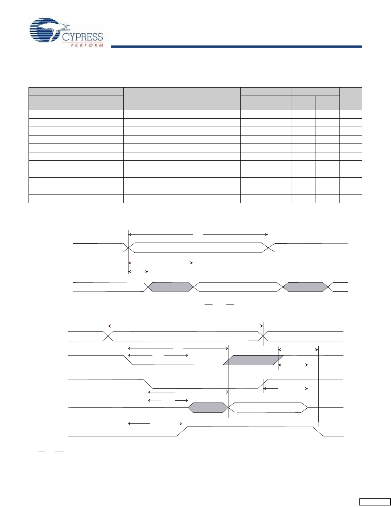
AC Switching Characteristics
SRAM Read Cycle
Parameter
Cypress
Parameter
Alt
tACE
tRC [6]
tAA [7]
tDOE
tOHA [7]
tLZCE [8]
tHZCE [8]
tLZOE [8]
tHZOE [8]
tPU [5]
tPD [5]
tELQV
tAVAV, tELEH
tAVQV
tGLQV
tAXQX
tELQX
tEHQZ
tGLQX
tGHQZ
tELICCH
tEHICCL
Switching Waveforms
Description
Chip Enable Access Time
Read Cycle Time
Address Access Time
Output Enable to Data Valid
Output Hold After Address Change
Chip Enable to Output Active
Chip Disable to Output Inactive
Output Enable to Output Active
Output Disable to Output Inactive
Chip Enable to Power Active
Chip Disable to Power Standby
25 ns
Min
Max
25
25
25
10
5
5
10
0
10
0
25
Figure 7. SRAM Read Cycle 1: Address Controlled [6, 7]
W5&
$''5(66
W$$
W2+$
'4
'$7$287
'$7$9$/,'
45 ns
Unit
Min Max
45
ns
45
ns
45
ns
20
ns
5
ns
5
ns
15
ns
0
ns
15
ns
0
ns
45
ns
Figure 8. SRAM Read Cycle 2: CE and OE Controlled [6]
$''5(66
&(
2(
'4
'$7$287
W5&
W/=&(
W$&(
W'2(
W/=2(
W3'
W+=&(
W+=2(
'$7$9$/,'
W38
,&&
67$1'%<
Notes
6. WE and HSB must be High during SRAM Read cycles.
7. Device is continuously selected with CE and OE both Low.
8. Measured ±200 mV from steady state output voltage.
$&7,9(
Document Number: 001-51000 Rev. **
Page 8 of 14
[+] Feedback
Share Link: 