SC1156SW.TR(2001) 데이터 시트보기 (PDF) - Semtech Corporation
부품명
상세내역
일치하는 목록
SC1156SW.TR
(Rev.:2001)
(Rev.:2001)
Semtech Corporation

SC1156SW.TR Datasheet PDF : 7 Pages
| |||
SC1156
POWER MANAGEMENT
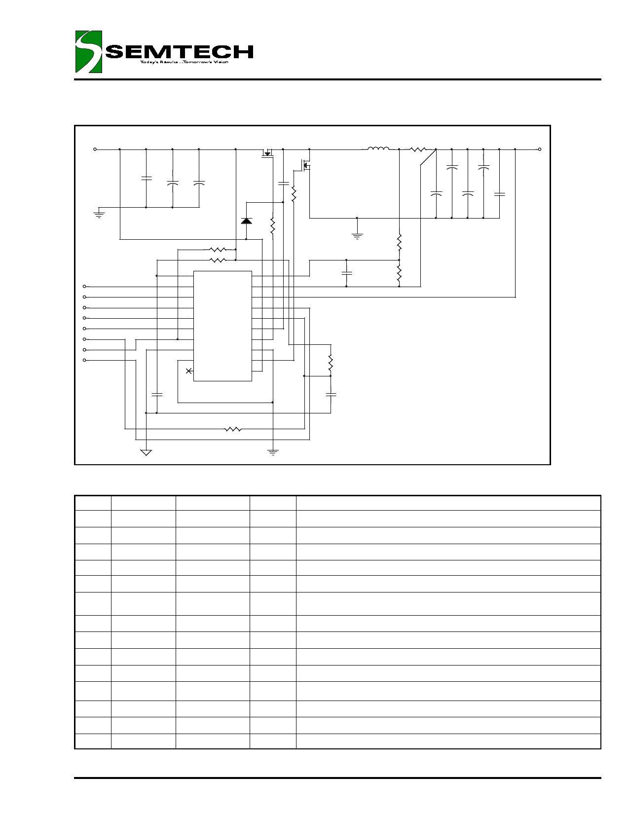
Block Diagram
VID4
VID3
VID2
VID1
VID0
VOSENSE
1.25V REF
D/A
PWRGOOD
OVP
OPEN
COLLECTORS
+
-
+
-
VCC
+
-
VCC CS- CS+
SHUTDOWN
70mV
CURRENT LIMIT
+
-
OSCILLATOR
R
Q
S
-
+
+
-
ERROR
AMP
GND
EN
LEVEL SHIFT
AND DRIVE
BSTH
DH
PGNDH
SHOOT-THRU
CONTROL
LOW SIDE
DRIVE
BSTDL
DL
PGNDL
Theory of Operation
The D/A Converter generates an output voltage determined
by an internal trimmed bandgap voltage reference and
the status of the VID0 through VID4 inputs. This voltage is
applied to the non-inverting input of the error amplifier,
the inverting input of the error amplifier is fed from the
VOSENSE pin via a precision resistor divider. The error
amplifier itself is a transconductance amplifier with an in-
ternal load resistor. The open loop gain is internally set to
approximately 40 dB.
The internal oscillator uses an on-chip capacitor and a
trimmed precision current source to set the frequency of
oscillation to 200 kHz. The triangular output of the oscil-
lator is compared to the output of the error amplifier. The
output of the PWM comparator is a pulse width modu-
lated signal whose duty cycle increases as the voltage at
the VOSENSE pin decreases.
The output of the current limit comparator goes high when
its input voltage exceeds approximately 70mV, this sets
the current limit latch, immediately terminating the cur-
rent ON time. The current limit latch is reset in the middle
of the OFF time when the triangular wave oscillator reaches
its highest point .
When the output of the PWM comparator is high, output
DH is driven high, provided that the VID code is valid, the
current limit latch has not been set and the Enable (EN)
pin is not pulled low. When the PWM comparator output is
low DL is always driven high.
The Shoot-through control circuitry modifies the DH and
DL waveforms slightly, ensuring that there is a short delay
between one turning OFF and the other turning ON. This
ensures that the ON times of the external FETs driven by
DH and DL do not overlap.
© 2000 Semtech Corp.
4
www.semtech.com
Share Link: