PI6C2408-6WIE 데이터 시트보기 (PDF) - Pericom Semiconductor Corporation
부품명
상세내역
일치하는 목록
PI6C2408-6WIE Datasheet PDF : 10 Pages
| |||
PI6C2408
Zero Delay Clock Buffer 1122334455667788990011223344556677889900112233445566778899001122112233445566778899001122334455667788990011223344556677889900112211223344556677889900112233445566778899001122334455667788990011221122334455667788990011223344556677889900112233445566778899001122112233445566778899001122
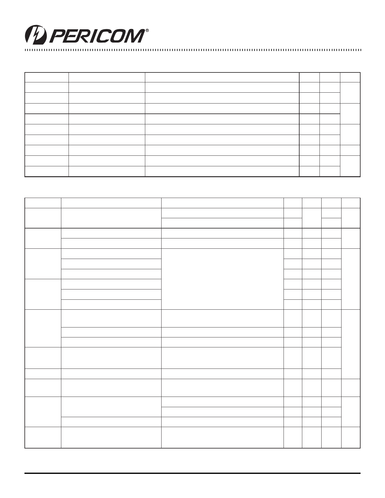
DC Electrical Characteristics for Commercial Temperature Devices
Parameter
Description
Test Conditions
VIL
VIH
IIL
IIH
VOL
VOH
IDD (PD mode)
IDD
IDD
Input LOW Voltage
Input HIGH Voltage
Input LOW Current
Input HIGH Current
Output LOW Voltage
Output HIGH Voltage
Power Down Supply Current
Supply Current
Supply Current
VIN = 0V
VIN = VDD
IOL = 8mA (–1, –2, –3,–4, –6); IOL = 12mA (–1H)
IOH = –8mA (–1, –2, –3,–4, –6); IOH = –12mA (–1H)
SEL1 = 0 (-1,-2,-3,-4,-1H); SEL2 = 0 (-6)
Unloaded outputs, 66.67 MHz, Select inputs at VDD or GND
Unloaded outputs 100 MHz Select Inputs @ VDD or GND
Min.
2.0
2.4
Max.
0.8
50
100
0.4
12
39
54
Units
V
µA
V
µA
mA
AC Electrial Characteristicsfor Commercial Temperature Device
Parameters
Name
Test Conditions
Min. Typ. Max. Units
FO
tDC
tR
tF
tSK(O)
t0
Output Frequency
30pF load
15pF load
Duty Cycle(1) (–1H)
Duty Cycle (–1, –2, –3, –4, –6)
Rise Time(1) @30pF
Measured at VDD/2, for high drive output
Measured at VDD/2, for normal drive output
Rise Time(1) @15pF
Rise Time(1) @30pF (–1H)
Fall Time(1) @30pF
Measured between 0.8V and 2.0V
Fall Time(1) @15pF
Fall Time(1) @30pF (–1H)
Output to Output Skew(1) within same
bank (–1,–1H,–2,–3,–4,–6)
All outputs equally loaded, VDD/2
OUTA to OUTB Skew(1) (–1,–1H,–4) All outputs equally loaded, VDD/2
OUTA to OUTB Skew(1) (–2,–3,–6) All outputs equally loaded, VDD/2
Input to Output Delay, CLKIN
Rising Edge to FB_IN Rising Edge(1)
Measured at VDD/2
10
100
140
MHz
45 50 55 %
40 50 60
2.2
1.5
1.5 ns
2.2
1.5
1.25
200
200
400 ps
0 ±150
tSK(D) Device to Device Skew(1)
Measured at VDD/2 on FB_IN pins of devices
tSLEW Output Slew Rate(1)
Measured between 0.8V and 2.0V on –1H
device using Test Circuit #2
1
tJIT
Cycle-to-Cycle Jitter (1)(–1,–1H,–4) Measured at 66.67 MHz, loaded 30pF outputs
Measured at 140 MHz, loaded 15pF outputs
Cycle-to-Cycle Jitter(1) (–2,–3,–6)
Measured at 66.7 MHz, loaded 30pF outputs
tLOCK PLL Lock Time(1)
Stable power supply, valid clocks
presented on CLKIN and FB_IN pins
0 500
V/ns
200
100 ps
400
1.0 ms
Notes:
1. See Switching Waveforms on page 7.
6
PS8589E 09/15/04
Share Link: 