MX98725 데이터 시트보기 (PDF) - Macronix International
부품명
상세내역
일치하는 목록
MX98725 Datasheet PDF : 33 Pages
| |||
MX98725
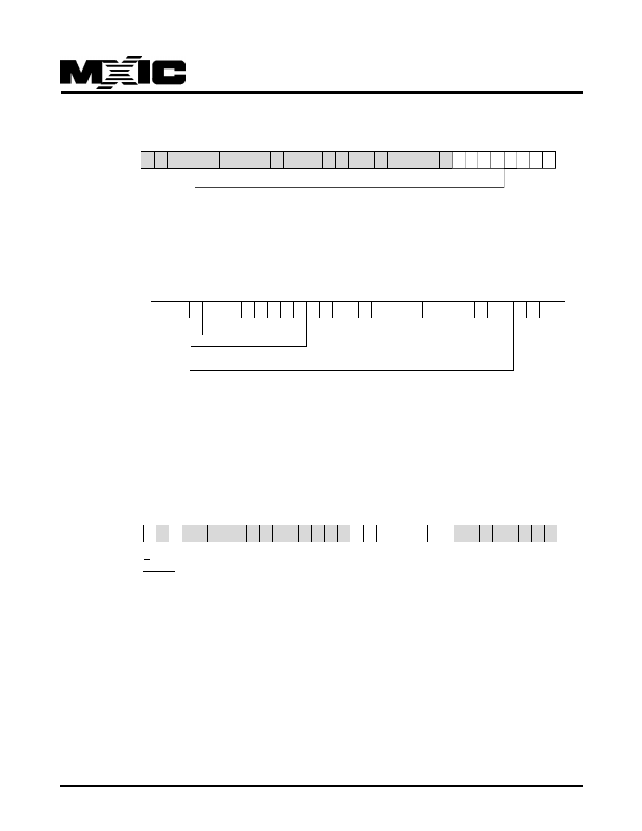
5.1.8 PCI CAPABILITY POINTER REGISTER ( PFCP ) ( Offset 37h-34h )
31 30 29 28 27 26 25 24 23 22 21 20 19 18 17 16 15 14 13 12 11 10 9 8 7 6 5 4 3 2 1 0
Capability Pointer (Set to 44h)
bit 7- 0 : Capability pointer (Cap_Ptr) is set to 44h if PMEB is connected to PCI bus, otherwise 00.
bit 31- 8 : reserved
5.1.9 INTERRUPT REGISTER ( PFIT ) ( Offset 3Fh-3Ch )
31 30 29 28 27 26 25 24 23 22 21 20 19 18 17 16 15 14 13 12 11 10 9 8 7 6 5 4 3 2 1 0
0 0111 000 000 01 00 0
Max_Lat
Min-Gnt
Interrupt Pin
Interrupt Line
bit 7 - 0 : Interrupt Line, system BIOS will writes the routing information into this field, driver can use this information
to determine priority and interrupt vector.
bit 15 - 8 : Interrupt Pin, fixed to 01h which use INTA#.
bit 31 - 24 : Max_Lat which is a maximum period for a access to PCI bus.
bit 23 - 16 : Min_Gnt which is the maximum period that MX98725 needs to finish a brust PCI cycle.
5.1.10 PCI DRIVER AREA REGISTER ( PFDA ) ( 43h-40h )
31 30 29 28 27 26 25 24 23 22 21 20 19 18 17 16 15 14 13 12 11 10 9 8 7 6 5 4 3 2 1 0
Sleep Mode
Board Type
Driver Special Use
bit 31 : Sleep Mode, set to sleep mode which allows access to PCI configuration space, a hardwarreset or reset to
this bit can exit from sleep mode. Magic packet can be received under sleep mode if CSR16<21> ( Magic
Packet Enable ) is set.
bit 30 : not used
bit 29 : board type
bit 15 - 8 : driver is free to read and write this field for any purpose.
bit 7 - 0 : not used.
P/N:PM0488
REV. 1.7, SEP. 15, 1998
9
Share Link: 