MC143416 데이터 시트보기 (PDF) - Freescale Semiconductor
부품명
상세내역
일치하는 목록
MC143416 Datasheet PDF : 24 Pages
| |||
Freescale Semiconductor, Inc.
FUNCTIONAL DESCRIPTION
CLOCK GENERATION
Introduction
The clock generation block generates all timing signals
necessary for the operation of the device from a crystal input
or alternatively from the oversampling clock (OSR CLK) sup-
plied through the MCLK input. The selection between these
two modes is controlled by the MCLK_SEL register.
The clock generation block generates the oversampling
clocks, the intermediate sampling clock (for internal use),
and the clocking signals for the SSI ports. The ratio of the
oversampling clock to the sampling clock defines the deci-
mation/interpolation rate. When the MCLK input is used, this
clock is the OSR clock. The bit clock for the Synchronous
Serial Interfaces (SSIs) is equal to the oversampling clock
frequency (fOSR).
Note that the MCLK and XTALin frequency need to be inte-
ger multiples of the codecs’ sampling rates.
Oversampling Clock Selection
The practical maximum and minimum oversampling ratio
at which the device will operate is determined by the hard-
ware implementation. At all times, the following conditions
need to be met for proper operation:
• Second order sigma–delta modulation is performed and
the oversampling ratio has to be kept in the range of 102
to 254 (LSDIV values 51 to 127).
• Oversampling frequency is limited to 4 MHz.
• The ratio of the oversampling clock to the system clock
should be greater than or equal to 7 when the
oversampling clock is derived from the crystal input, and
greater than or equal to 8 when derived from the MCLK
input.
• The system clock should provide a minimum of 580
cycles per sampling period per codec. For example, the
Fmin value of two codecs running at 8 ks/s would be:
Fmin = FS * 580 * 2 = 8000 * 580 * 2 = 9.28 MHz
• The maximum crystal frequency and operating system
clock frequency is 30 MHz.
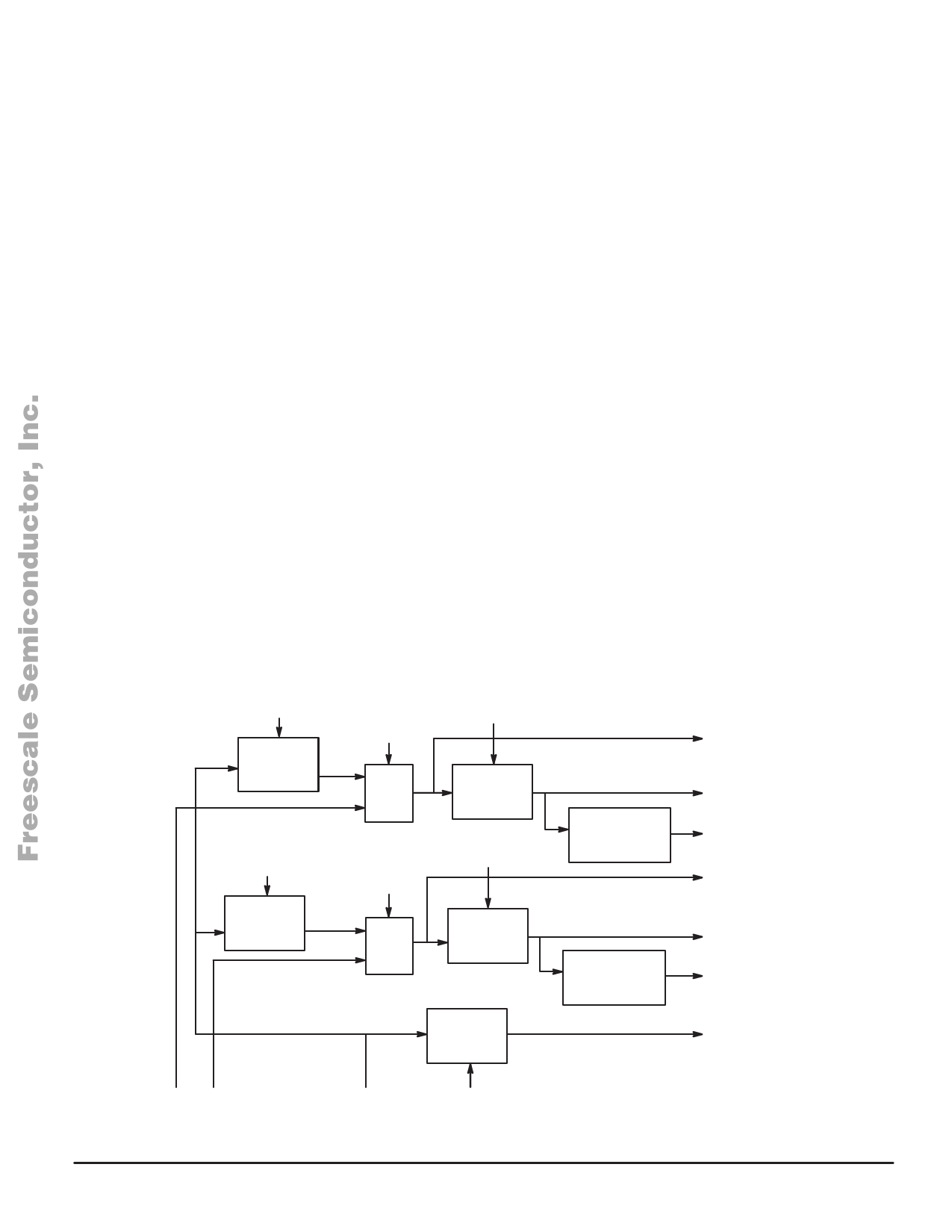
Clock Generation and Divide Ratios
The functional block diagram is shown in Figure 3.
HSDIV and LSDIV Ratios. The clock generation block
contains separate programmable divisors for each codec.
The relationship of XTALin frequency, the dividers, and the
sampling frequency (FS) is:
XTALin = 2 * FS * (HSDIV * LSDIV)
where HSDIV = 7, 8, ..., 63 (default 16), and LSDIV = 51,
..., 127 (default 51).
When the signal is a MCLK input only, the LSDIV value ap-
plies; the HSDIV setting is a don’t care. Higher settings will
positively impact (reduce) power consumption.
Tables 2 through 5 provide examples of the divisor values
to derive the OSR and FS from several different crystal val-
ues.
System Divide Ratios. The system clock frequency has
to be set to a minimum of seven times the oversampling fre-
quency of the codec running the maximum OSR. This is ac-
complished when clocking is derived from the crystal when
the HSDIV0 and HSDIV1 values are set to 7 or more. When
clocking is derived from MCLK0 and/or MCLK1, a minimum
ratio of 8 has to be guaranteed between any MCLK and the
XTALin frequency.
HSDIV0 (5:0)
HSDIV
CLKSEL0
MUX
LSDIV0 (6:0)
LSDIV
HSDIV1 (5:0)
HSDIV
CLKSEL1
MUX
LSDIV1 (6:0)
LSDIV
DIV1,
2, 3/2, 3
FRAME SYNC
GENERATOR
FRAME SYNC
GENERATOR
CODEC 0 OSR CLOCK
AND SSI0 BIT CLOCK
CODEC 0
INTERMEDIATE
SAMPLING CLOCK
SSI0 FRAME SYNC
CODEC 1 OSR CLOCK
AND SSI1 BIT CLOCK
CODEC 1
INTERMEDIATE
SAMPLING CLOCK
SSI1 FRAME SYNC
SYSTEM CLOCK
MCLK0 MCLK1
MOTOROLA
XTALin
SYS_DIV (1:0)
Figure 3. Block Diagram of the Clock Generation Scheme
For More Information On This Product,
Go to: www.freescale.com
MC143416
9
Share Link: 