MAX8834Y 데이터 시트보기 (PDF) - Maxim Integrated
부품명
상세내역
일치하는 목록
MAX8834Y Datasheet PDF : 44 Pages
| |||
MAX8834Y/MAX8834Z
Adaptive Step-Up Converters
with 1.5A Flash Driver
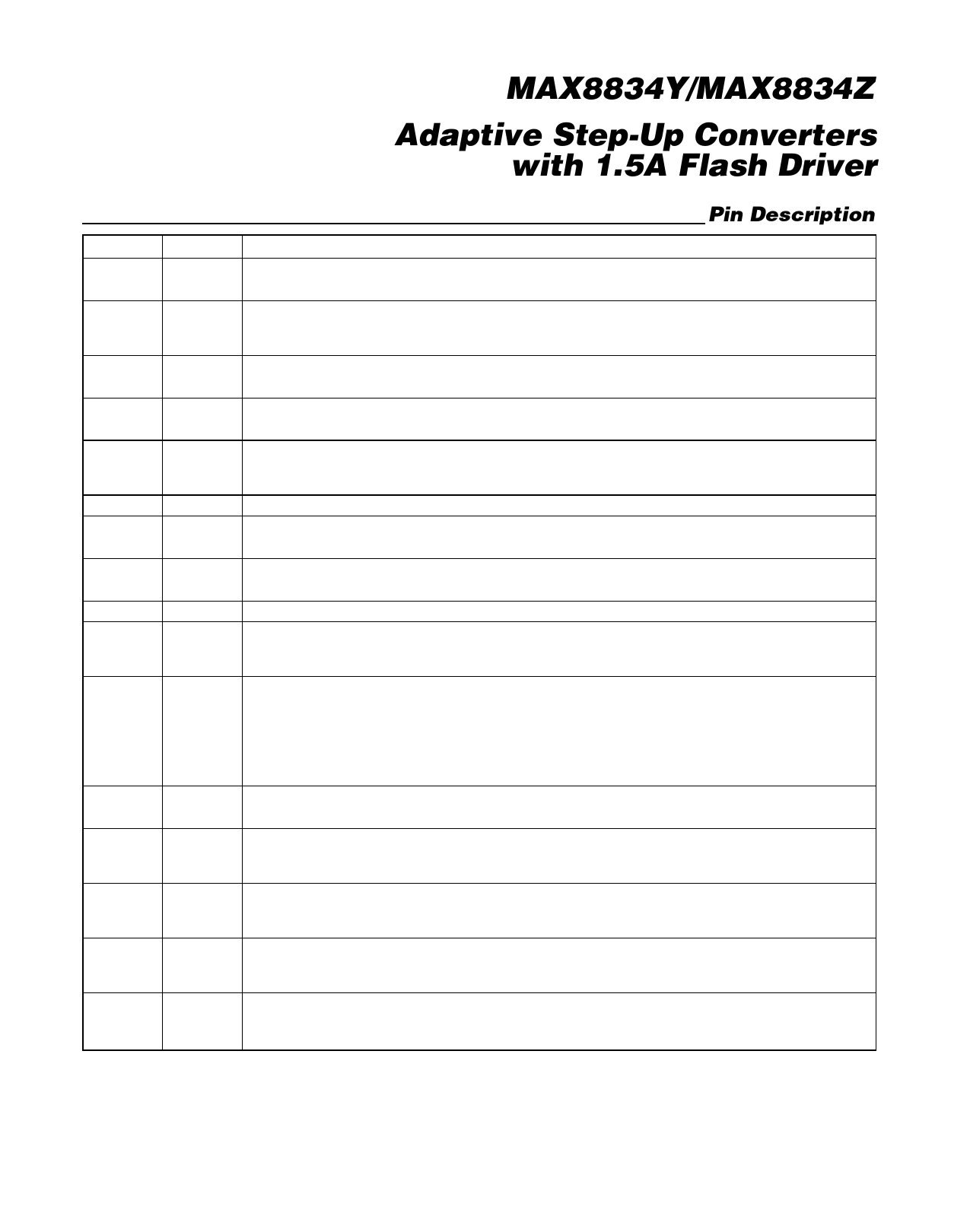
PIN
A1, B1
A2, B2
A3, B3
A4
A5
B4
B5
C1
C2, D2
C3
C4
C5
D1
D3
D4
D5
Pin Description
NAME
OUT
LX
PGND
IN
VDD
SCL
AGND
COMP
FGND
LED_EN
GSMB
SDA
FLED2
FLED1
INDLED
NTC
FUNCTION
Regulator Output. Connect OUT to the anodes of the external LEDs. Bypass OUT to PGND with a 10µF
ceramic capacitor. OUT is connected to LX through an internal 10k resistor during shutdown.
Inductor Connection. Connect LX to the switched side of the inductor. LX is internally connected to
the drains of the internal MOSFETs. LX is connected to OUT through an internal 10k resistor during
shutdown.
Power Ground. Connect PGND to AGND and to the input capacitor ground. Connect PGND to the PCB
ground plane.
Analog Supply Voltage Input. The input voltage range is 2.5V to 5.5V. Bypass IN to AGND and PGND
with a 10µF ceramic capacitor as close as possible to the IC. IN is high impedance during shutdown.
Logic Input Supply Voltage. Connect VDD to the logic supply driving SCL, SDA, LED_EN, and GSMB.
Bypass VDD to AGND with a 0.1µF ceramic capacitor. When VDD is below the UVLO, the I2C registers
reset and the step-up converter turns off.
I2C Clock Input. Data is read on the rising edge of SCL.
Analog Ground. Connect AGND to PGND and to the input capacitor ground. Connect AGND to the PCB
ground plane.
Compensation Input. See the Compensation Network Selection section for details. COMP is internally
pulled to AGND through a 180 resistor in shutdown.
FLED1/FLED2 and INDLED Power Ground. Connect FGND to PGND.
LED Enable Logic Input. LED_EN controls FLED1, FLED2, and INDLED, depending on control bits
written into the LED_CNTL register. See the LED_EN Control register description for an explanation of
this input function. LED_EN has an internal 800k pulldown resistor to AGND.
GSM Blank Signal. Assert GSMB to reduce the current regulator settings according to the values
programmed into the GSMB_CUR register. The status of the flash safety timer and the flash/movie
mode values in the current regulator registers are not affected by the GSMB state. Connect GSMB to
the PA module enable signal or other suitable logic signal that indicates a GSM transmit is in
process. Polarity of this signal is set by a bit in the GSMB_CUR register (default is active-high).
GSMB has an internal 800k pulldown resistor to AGND.
I2C Data Input. Data is read on the rising edge of SCL and data is clocked out on the falling edge of
SCL.
FLED2 Current Regulator. Current flowing into FLED2 is based on the internal I2C registers
FLASH2_CUR and MOVIE_CUR. Connect FLED2 to the cathode of an external flash LED or LED
module. FLED2 is high impedance during shutdown. If unused, connect FLED2 to ground.
FLED1 Current Regulator. Current flowing into FLED1 is based on the internal I2C registers
FLASH1_CUR and MOVIE_CUR. Connect FLED1 to the cathode of an external flash LED or LED
module. FLED1 is high impedance during shutdown. If unused, connect FLED1 to ground.
INDLED Current Regulator. Current flowing into INDLED is based on the internal I2C registers
IND_CUR. Connect INDLED to the cathode of an external indicator LED. INDLED is high impedance
during shutdown. If unused, connect INDLED to ground.
NTC Bias Output. NTC provides 20µA to bias the NTC thermistor. The NTC voltage is compared to the
trip threshold programmed by the NTC_CNTL register. NTC is high impedance during shutdown.
Connect NTC to IN if not used. See the Finger-Burn Protection (NTC) section for details.
Maxim Integrated
11
Share Link: 