MAX780ACAG 데이터 시트보기 (PDF) - Maxim Integrated
부품명
상세내역
일치하는 목록
MAX780ACAG Datasheet PDF : 12 Pages
| |||
Dual-Slot PCMCIA Analog Power Controller
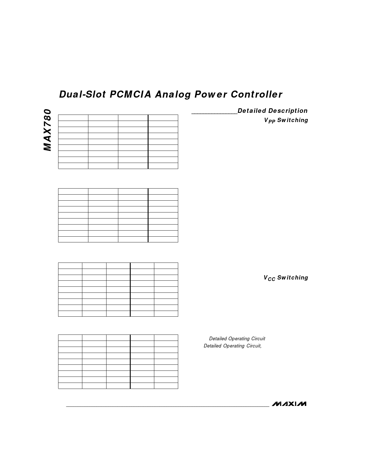
Table 1. AVPP Control Logic
C1
AVPP1
AVPP0
0
0
0
0
0
1
0
1
0
0
1
1
1
0
0
1
0
1
1
1
0
1
1
1
Table 2. BVPP Control Logic
C1
BVPP1
BVPP0
0
0
0
0
0
1
0
1
0
0
1
1
1
0
0
1
0
1
1
1
0
1
1
1
AVPP
0V
VCCIN
VPPIN
High-Z
0V
0V
VCCIN
VPPIN
BVPP
0V
VCCIN
VPPIN
High-Z
0V
0V
VCCIN
VPPIN
Table 3. ADRV3 and ADRV5 Control Logic
C1
AVCC1 AVCC0 ADRV3 ADRV5
0
0
0
0V
0V
0
0
1
Hi-Z
0V
0
1
0
0V
Hi-Z
0
1
1
0V
0V
1
0
0
0V
0V
1
0
1
0V
0V
1
1
0
0V
Hi-Z
1
1
1
Hi-Z
0V
Table 4. BDRV3 and BDRV5 Control Logic
C1
BVCC1 BVCC0 BDRV3 BDRV5
0
0
0
0V
0V
0
0
1
Hi-Z
0V
0
1
0
0V
Hi-Z
0
1
1
0V
0V
1
0
0
0V
0V
1
0
1
0V
0V
1
1
0
0V
Hi-Z
1
1
1
Hi-Z
0V
________________Detailed Description
VPP Switching
All four versions (A, B, C, and D) of the MAX780 allow
simple switching of PCMCIA card VPP to 0V, 5V, and
12V. On-chip power MOSFETs connect AVPP and
BVPP to either GND, VCCIN, or VPPIN. The AVPP0
and AVPP1 control logic inputs determine the state of
AVPP. Likewise, BVPP0 and BVPP1 control BVPP.
To prevent VPP overshoot due to parasitic inductance
in the +12V supply, the VPPIN bypass capacitor (CIN)
should be 10 times greater than the capacitance from
AVPP (CA) or BVPP (CB) to GND. Hence, when CA
and CB are 0.1µF, CIN should be 1.0µF.
The AGPI and BGPI status outputs signal when the VPP
lines are valid. AGPI goes low when AVPP exceeds
11.05V; BGPI goes low when BVPP exceeds 11.05V.
The status outputs and the reference are only active
when SHDN is high.
Pulling SHDN low puts the MAX780 into a low supply-
current mode and disables the reference and the AGPI
and BGPI status outputs. The VCC level shifters
ADRV5, ADRV3, BDRV5, BDRV3 are all forced low
when SHDN is low. VPP switching is not affected by the
state of SHDN. Program AVPP and BVPP to 0V for low-
est power consumption when SHDN is low. Wait at
least 200µs after bringing the MAX780 out of shutdown
before checking AGPI or BGPI since the reference
needs time to stabilize.
VCC Switching
The MAX780 contains level shifters that simplify driving
external power MOSFETs to switch PCMCIA card VCC
to 3.3V and 5V. While a PCMCIA card is being insert-
ed into the socket, the VCC pins on the card edge con-
nector should be powered down to 0V so that “hot
insertion” does not damage the PCMCIA card. The
simplest way to accomplish this is to pull out a
mechanical switch before the PCMCIA card is inserted.
The mechanical switch can be pushed in only when
the card has been fitted snugly into its socket. The
MAX780 Detailed Operating Circuit shows this method.
In the Detailed Operating Circuit, (with the mechanical
interlock switch closed) the PCMCIA card VCC cannot
be pulled more than a diode drop below 3.3V. The N-
channel power MOSFET that connects VCC to 3.3V has
its drain tied to VCC and its source tied to 3.3V, so that
its body diode prevents the card’s VCC from falling to
0V. If it were rotated so that the source connected to
VCC, then applying 5V to VCC would short the 5V sup-
ply to the 3.3V supply via the MOSFET’s body diode.
6 _______________________________________________________________________________________
Share Link: 