MAX7400 데이터 시트보기 (PDF) - Maxim Integrated
부품명
상세내역
일치하는 목록
MAX7400 Datasheet PDF : 12 Pages
| |||
8th-Order, Lowpass, Elliptic,
Switched-Capacitor Filters
RIPPLE
VSUPPLY
fC
TRANSITION RATIO =
fS
fC
fS
PASSBAND
STOPBAND
fC fS
FREQUENCY
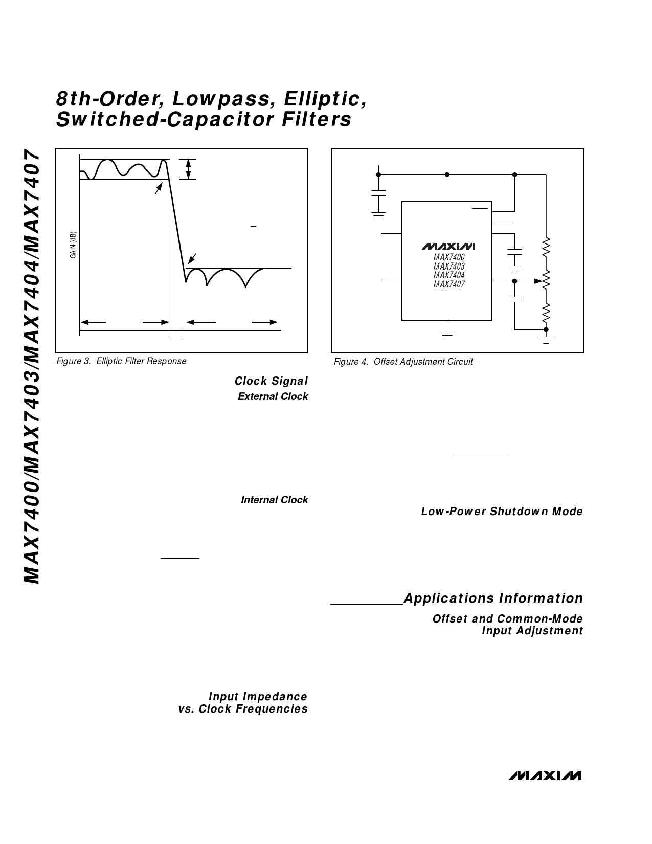
Figure 3. Elliptic Filter Response
Clock Signal
External Clock
The MAX7400/MAX7403/MAX7404/MAX7407 SCFs
were designed for use with external clocks that have a
40% to 60% duty cycle. When using an external clock,
drive CLK with a CMOS gate powered from 0 to VDD.
Varying the rate of the external clock adjusts the filter
corner frequency:
fC = fCLK / 100
Internal Clock
When using the internal oscillator, the capacitance
(COSC) on the CLK pin determines the oscillator fre-
quency:
⋅ fOSC (kHz) =
K 103 ;
COSC
COSC
in pF
where K = 38 for the MAX7400/MAX7403, and K = 34
for the MAX7404/MAX7407. Since the capacitor value
is in picofarads, minimize the stray capacitance at CLK
so that it does not affect the internal oscillator frequen-
cy. Varying the rate of the internal oscillator adjusts the
filter’s corner frequency by a 100:1 clock-to-corner fre-
quency ratio. For example, an internal oscillator fre-
quency of 100kHz produces a nominal corner
frequency of 1kHz.
Input Impedance
vs. Clock Frequencies
The MAX7400/MAX7403/MAX7404/MAX7407’s input
impedance is effectively that of a switched-capacitor
resistor and is inversely proportional to frequency. The
0.1µF
INPUT
CLOCK
VDD
SHDN
OUT
OUTPUT
IN
COM
0.1µF
50k
MAX7400
MAX7403
CLK
MAX7404
MAX7407
OS
50k
0.1µF
GND
50k
Figure 4. Offset Adjustment Circuit
input impedance determined by the following equation
represents the average input impedance, since the
input current is not continuous. As a rule, use a driver
with an output source impedance less than 10% of the
filter’s input impedance. Estimate the input impedance
of the filter using the following formula:
⋅ ZIN(Ω)
=
1
(fCLK CIN)
where fCLK = clock frequency and CIN = 0.85pF.
Low-Power Shutdown Mode
These devices feature a shutdown mode that is activat-
ed by driving SHDN low. Placing the filter in shutdown
mode reduces the supply current to 0.2µA (typ) and
places the output of the filter into a high-impedance
state. For normal operation, drive SHDN high or con-
nect to VDD.
Applications Information
Offset and Common-Mode
Input Adjustment
The voltage at COM sets the common-mode input volt-
age and is internally biased at midsupply by a resistor-
divider. Bypass COM with a 0.1µF capacitor and
connect OS to COM. For applications requiring offset
adjustment or DC level shifting, apply an external bias
voltage through a resistor-divider network to OS, as
shown in Figure 4. (Note: Do not leave OS unconnect-
ed.) The output voltage is represented by the following
equation:
VOUT = (VIN - VCOM) + VOS
10 ______________________________________________________________________________________
Share Link: 