MAX7401 데이터 시트보기 (PDF) - Maxim Integrated
부품명
상세내역
일치하는 목록
MAX7401 Datasheet PDF : 12 Pages
| |||

8th-Order, Lowpass, Bessel,
Switched-Capacitor Filters
A switched-capacitor filter such as the MAX7401/
MAX7405 emulates a passive ladder filter. The filter’s
component sensitivity is low when compared to a cas-
caded biquad design because each component affects
the entire filter shape, not just one pole-zero pair. In other
words, a mismatched component in a biquad design will
have a concentrated error on its respective poles, while
the same mismatch in a ladder filter design results in an
error distributed over all poles.
Clock Signal
External Clock
The MAX7401/MAX7405 family of SCFs is designed for
use with external clocks that have a 40% to 60% duty
cycle. When using an external clock with these devices,
drive CLK with a CMOS gate powered from 0 to VDD.
Varying the rate of the external clock adjusts the corner
frequency of the filter as follows:
fC = fCLK / 100
Internal Clock
When using the internal oscillator, connect a capacitor
(COSC) between CLK and ground. The value of the
capacitor determines the oscillator frequency as follows:
⋅ fOSC (kHz) =
K 103
C OSC
; COSC in pF
where K = 38 for MAX7401 and K = 34 for MAX7405.
Minimize the stray capacitance at CLK so that it does
not affect the internal oscillator frequency. Vary the rate
of the internal oscillator to adjust the filter’s corner fre-
quency by a 100:1 clock-to-corner frequency ratio. For
example, an internal oscillator frequency of 100kHz
produces a nominal corner frequency of 1kHz.
Input Impedance vs. Clock Frequencies
The MAX7401/MAX7405’s input impedance is effectively
that of a switched-capacitor resistor and is inversely pro-
portional to frequency. The input impedance values
determined below represent the average input imped-
ance since the input current is not continuous. As a rule,
use a driver with an output impedance less than 10% of
the filter’s input impedance. Estimate the input imped-
ance of the filter using the following formula:
( ) ⋅ ZIN =
1
fCLK CIN
where fCLK = clock frequency and CIN = 3.37pF.
Low-Power Shutdown Mode
These devices feature a shutdown mode that is activat-
ed by driving SHDN low. In shutdown mode, the filter’s
supply current reduces to 0.2µA (typ) and its output
becomes high impedance. For normal operation, drive
SHDN high or connect to VDD.
___________Applications Information
Offset and Common-Mode
Input Adjustment
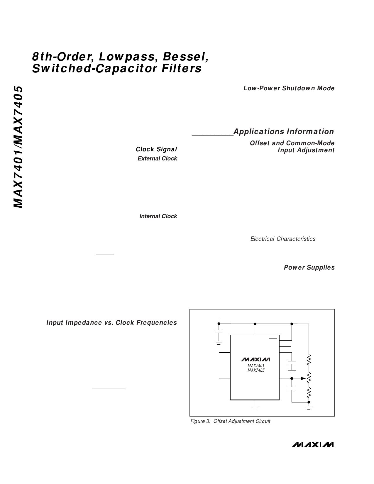
The voltage at COM sets the common-mode input volt-
age and is biased at mid-supply with an internal resistor-
divider. Bypass COM with a 0.1µF capacitor and
connect OS to COM. For applications requiring offset
adjustment or DC level shifting, apply an external bias
voltage through a resistor-divider network to OS, as
shown in Figure 3. (Note: Do not leave OS unconnect-
ed.) The output voltage is represented by this equation:
VOUT = (VIN - VCOM) + VOS
with VCOM = VDD / 2 (typical), and where (VIN - VCOM) is
lowpass filtered by the SCF, and VOS is added at the
output stage. See the Electrical Characteristics for the
voltage range of COM and OS. Changing the voltage on
COM or OS significantly from mid-supply reduces the fil-
ter’s dynamic range.
Power Supplies
The MAX7401 operates from a single +5V supply, and
the MAX7405 operates from a single +3V supply.
Bypass VDD to GND with a 0.1µF capacitor. If dual sup-
plies are required (±2.5V for MAX7401, ±1.5V for
MAX7405), connect COM to system ground and connect
VSUPPLY
0.1µF
INPUT
CLOCK
VDD
SHDN
OUT
OUTPUT
IN
COM
0.1µF
50k
MAX7401
MAX7405
CLK
OS
50k
0.1µF
50k
GND
Figure 3. Offset Adjustment Circuit
8 _______________________________________________________________________________________