LX8585-00 데이터 시트보기 (PDF) - Microsemi Corporation
부품명
상세내역
일치하는 목록
LX8585-00 Datasheet PDF : 8 Pages
| |||
PRODUCT DATABOOK 1996/1997
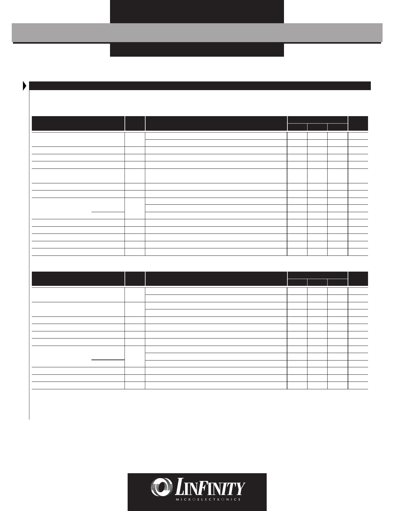
LX8585-xx/8585A-xx
4.6A LOW DROPOUT POSITIVE REGULATORS
PR O D U C T I O N D ATA S H E E T
ELECTRICAL CHARACTERISTICS
(Unless otherwise specified, these specifications apply over the operating ambient temperatures for the LX8585-xxC/85A-xxC with 0°C ≤ TA ≤ 125°C;
VIN - VOUT = 3V; IOUT = 4.6A. Low duty cycle pulse testing techniques are used which maintains junction and case temperatures equal to the ambient temperature.)
LX8585-00 / 8585A-00 (Adjustable)
Parameter
Symbol
Test Conditions
LX8585/85A-00
Units
Min. Typ. Max.
Reference Voltage
LX8585/85A
VREF IOUT = 10mA, TA = 25°C
10mA ≤ IOUT ≤ 4.6A, 1.5V ≤ (VIN - VOUT), VIN ≤ 7V, P ≤ PMAX
Line Regulation (Note 2)
∆VREF (VIN) IOUT = 10mA, 1.5V ≤ (VIN - VOUT), VIN ≤ 7V
Load Regulation (Note 2)
∆VREF (IOUT) VIN - VOUT = 3V, 10mA ≤ IOUT ≤ 4.6A
Thermal Regulation
∆VOUT(Pwr) TA = 25°C, 20ms pulse
Ripple Rejection (Note 3)
VOUT = 3.3V, f =120Hz, COUT = 100µf Tantalum, VIN = 5V
CADJ = 10µF, TA = 25°C, IOUT = 4.6A
Adjust Pin Current
IADJ
Adjust Pin Current Change
∆IADJ 10mA ≤ IOUT ≤ 4.6A, 1.5V ≤ (VIN - VOUT), VIN ≤ 7V
Dropout Voltage
LX8585
∆V ∆VREF = 1%, IOUT = 4.6A
∆VREF = 1%, IOUT = 3A
LX8585A
∆VREF = 1%, IOUT = 4.6A
Minimum Load Current
IOUT(MIN) VIN ≤ 7V
Maximum Output Current (Note 4)
IOUT(MAX) 1.4V ≤ (VIN - VOUT), VIN ≤ 7V
Temperature Stability (Note 3)
∆VOUT(t)
Long Term Stability (Note 3)
∆VOUT (t) TA = 125°C, 1000 hrs
RMS Output Noise (% of VOUT) (Note 3) VOUT (RMS) TA = 125°C, 10Hz £ f £ 10kHz
1.238
1.225
60
1.250
1.250
0.035
0.1
0.01
83
1.262
1.275
0.2
0.5
0.02
V
V
%
%
%/W
dB
55 100 µA
0.2
5
µA
1.2 1.4
V
1.1 1.3
V
1.1 1.2
V
2
10
mA
4.6
6
A
0.25
%
0.3
1
%
0.003
%
LX8585-15 / 8585A-15 (1.5V Fixed)
Parameter
Symbol
Test Conditions
Output Voltage (Note 4)
VOUT VIN = 5V, IOUT = 0mA, TA = 25°C
4.75V ≤ VIN ≤ 10V, 0mA ≤ IOUT ≤ 7A, TA = 25°C, P ≤ PMAX
Line Regulation (Note 2)
∆VOUT 4.75V ≤ VIN ≤ 7V
(VIN) 4.75V ≤ VIN ≤ 10V
Load Regulation (Note 2)
∆VOUT (IOUT) VIN = 5V, 10mA ≤ IOUT ≤ IOUT (MAX)
Thermal Regulation (Note 3)
∆VOUT(Pwr) TA = 25°C, 20ms pulse
Ripple Rejection (Note 3)
COUT = 100µF (Tantalum), IOUT = 4.6A, TA = 25°C
Quiescent Current
IQ
0mA ≤ IOUT ≤ IOUT (MAX) , 4.75V ≤ VIN ≤ 10V
Dropout Voltage
LX8585-15
∆V
∆VOUT = 1%, IOUT ≤ IOUT (MAX) , VIN - VOUT ≤ 7V
∆VOUT = 1%, IOUT ≤ 3A, VIN - VOUT ≤ 7V
LX8585A-15
∆VOUT = 1%, IOUT ≤ IOUT (MAX) , VIN - VOUT ≤ 7V
Temperature Stability (Note 3)
∆VOUT (T)
Long Term Stability (Note 3)
∆VOUT (t) TA = 125°C, 1000 hours
RMS Output Noise (% of VOUT) (Note 3) VOUT (RMS) TA = 25°C, 10Hz ≤ f ≤ 10kHz
LX8585/85A-15
Min. Typ. Max.
1.485
1.470
65
1.50
1.50
1
1
2.5
0.01
83
4
1.2
1.1
1.1
0.25
0.3
0.003
1.515
1.530
3
5
7
0.02
10
1.4
1.3
1.2
1
Units
V
V
mV
mV
mV
%/W
dB
mA
V
V
V
%
%
%
Note 2.
Note 3.
Note 4.
Regulation is measured at constant junction temperature, using pulse testing with a low duty cycle. Changes in output voltage due to heating
effects are covered under the specification for thermal regulation.
These parameters, although guaranteed, are not tested in production.
IOUT (MAX) is measured under the condition that VOUT is forced below its nominal value by 100mV.
Copyright © 1997
Rev. 2.2 12/97
3
Share Link: 