JBT6K47-AS 데이터 시트보기 (PDF) - Toshiba
부품명
상세내역
일치하는 목록
JBT6K47-AS Datasheet PDF : 22 Pages
| |||
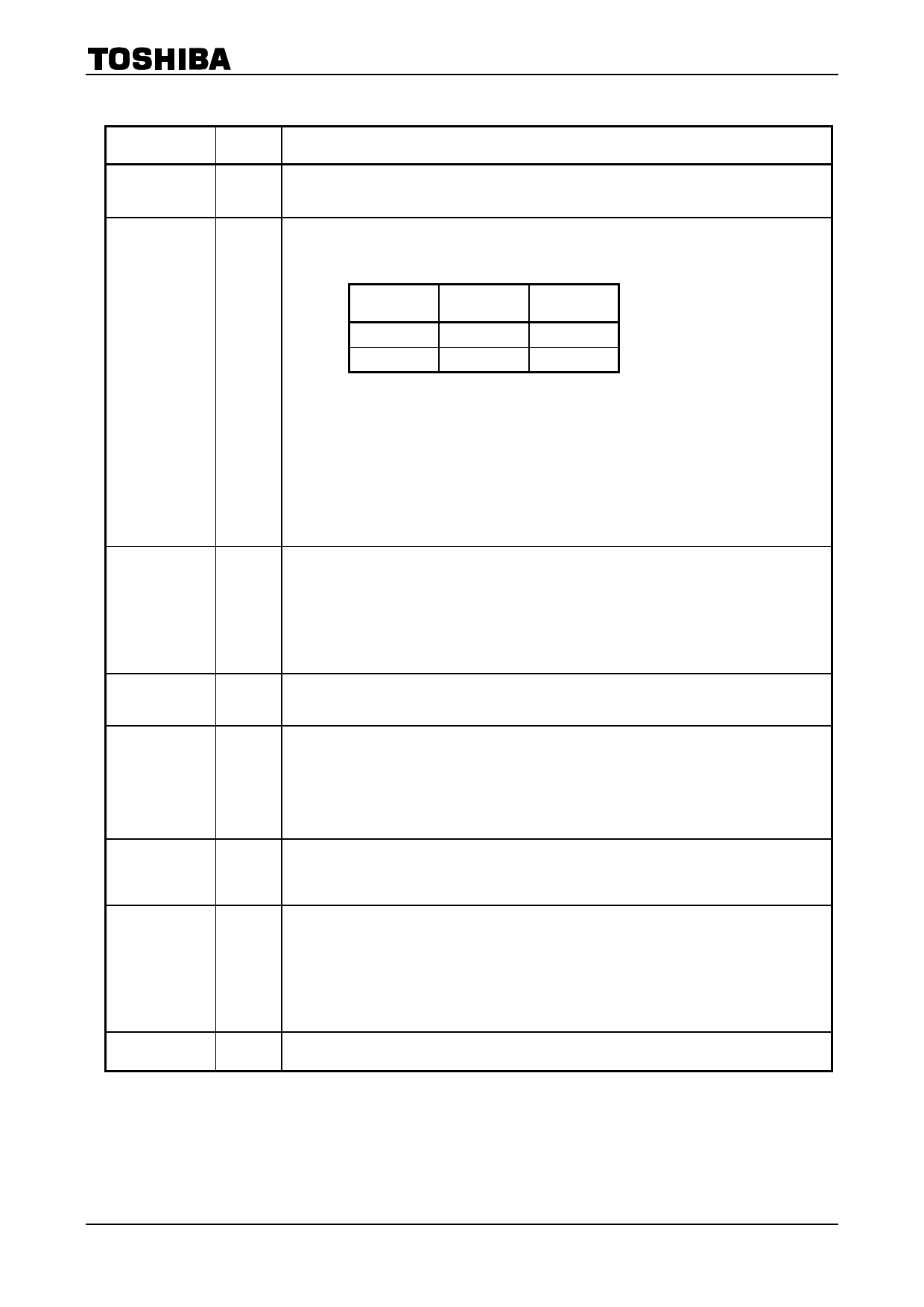
Pin Function
Pin Name
X01 to X88
Y01 to Y88
Z01 to Z88
DI/O
DO/I
U/D
CPH
XIN0 to XIN5
YIN0 to YIN5
ZIN0 to ZIN5
LOAD
POL
DW
JBT6K47-AS
I/O
Function
O
LCD panel drive pins
Data transfer enable pin
These pins indicate the input, starting to transfer the grayscale data, and the output, ending to
transfer the data. The U/D pin as shown below determines the function.
U/D
DI/O
DO/I
H
Input
Output
L
Output
Input
I/O
When set for input
A high on DI/O or DO/I is latched into the internal logic synchronously with the rising edge
of CPH. When the internal circuit is in standby state, the device is ready to transfer data.
The grayscale data is latched in sequentially, starting at the next rise of CPH. Also, regardless
how many rising edges are existed, DI/O or DO/I recognizes the first rising edge, and the
grayscale data is latched at the next rising edge.
When set for output
The pin is used to transfer the enable signal to the JBT6K47-AS at the next stage of the LCD
driver.
The pin enters standby state after outputting a high.
Transfer direction select pin
This pin specifys the directions of transfering the grayscale data.
Data is transferred synchronously with each rising edge of CPH in one of the following
sequences:
I
When U/D is High: X01 to Z01, X02 to Y02, Z03 to Z03, ……
When U/D is Low: X88 to Z88, X87 to Z87, X86 to Z86, ……
The voltage applied to this pin must be a DC-level voltage that is either high or low.
Data transfer clock pin (Can be stopped except the sampling period)
I
This clock input is used to transfer grayscale data.
In sync with the rising edge of CPH, writes grayscale data bus data to the sampling register.
Grayscale data input pin
An output data consists of six bits, and three output data are latched into the devise
simultaneously in one transfer. The POL pin and the result of the operation are written in this
I
data bus. Weighted data bit is shown below.
Grayscale data = (32 ´ wIN5) + (16 ´ wIN4) + (8 ´ wIN3) + (4 ´ wIN2) + (2 ´ wIN1) + wIN0
w = X, Y, Z
Data load input pin
I
This pin recognizes the High level. The data is transferred from the Sampling register to the
Load register asynchronously at the rising edge of CPH, and outputs the corresponded voltage
to the grayscale data.
Data polarity reversal pin
This pin is used to select reversing the grayscale data or not.
When POL is High: Reversing the grayscale data.
I
When POL is Low: Not reversing the grayscale data. The data is transferred to the internal logic
from the timing generator.
The grayscale data bus and the operation result of this pin are latched into the internal logic
synchronously with the rising edge of CPH.
I
Data control pin
This pin is used to forcibly make the grayscale data to High level.
9
2002-01-30
Share Link: 