IN74HC4094A 데이터 시트보기 (PDF) - IK Semicon Co., Ltd
부품명
상세내역
일치하는 목록
IN74HC4094A
IK Semicon Co., Ltd

IN74HC4094A Datasheet PDF : 8 Pages
| |||
TECHNICAL DATA
IN74HC4094A
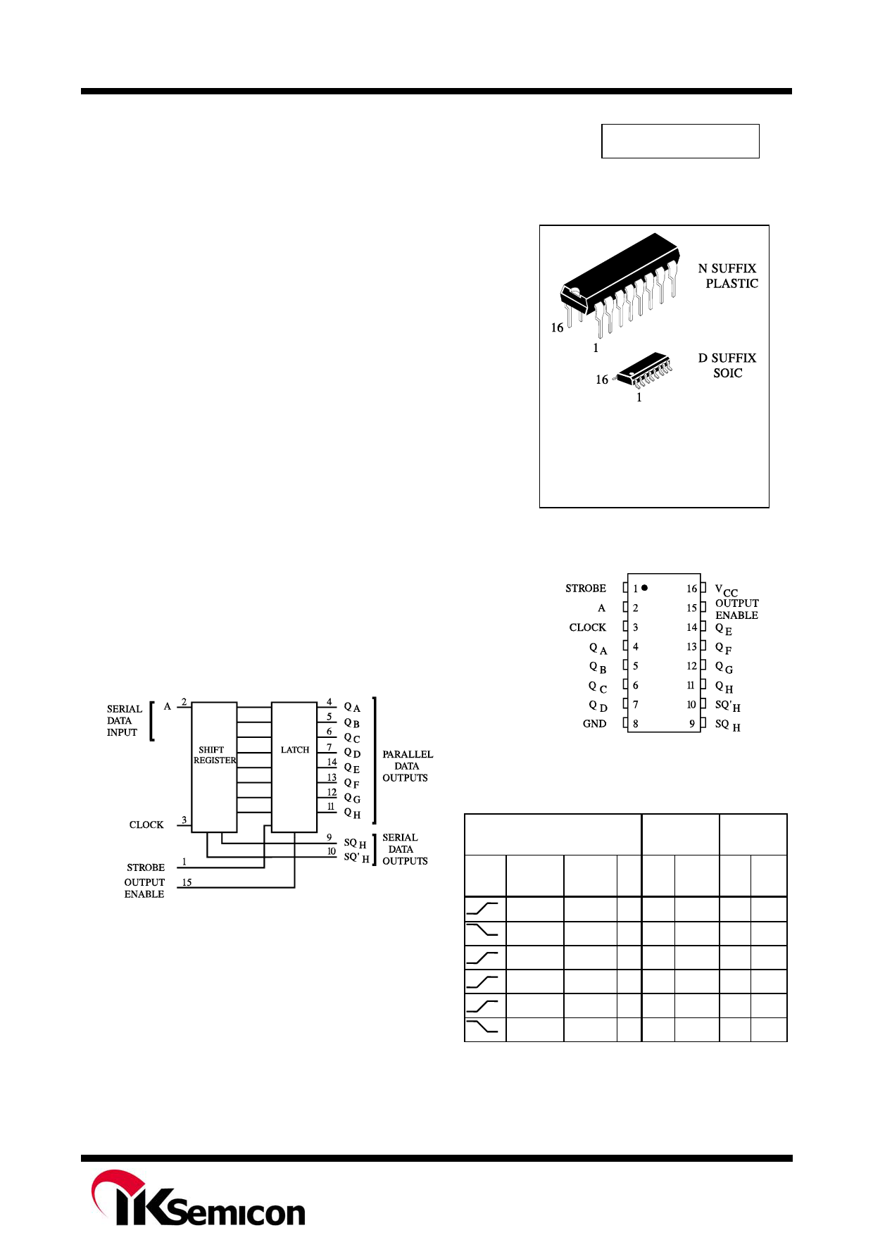
8-Bit Serial-Input Shift Register
With Latched 3-State Outputs
High-Performance Silicon-Gate CMOS
The IN74HC4094A is identical in pinout to the LS/ALS4094. The
device inputs are compatible with standard CMOS outputs; with pullup
resistors, they are compatible with LS/ALSTTL outputs.
This device consists of an 8-bit shift register and 8-bit D-type latch
with three-state parallel outputs. Data is shifted serially through the shift
register on the positive going transition of the clock input signal. The
output of the last stage SQH can be used to cascade several devices.
Data on the SQH output is transferred to a second output (SQH’) on the
following negative transition of the clock input signal. The data of each
stage of the shift register is provided with a latch, which latches data on
the negative going transition of the Strobe input signal. When the Strobe
input is held high, data propagates through the latch to a 3-state output
buffer.
This buffer is enabled when Output Enable input is taken high.
• Outputs Directly Interface to CMOS, NMOS, and TTL
• Operating Voltage Range: 2.0 to 6.0 V
• Low Input Current: 1.0 μA
• High Noise Immunity Characteristic of CMOS Devices
ORDERING INFORMATION
IN74HC4094AN Plastic
IN74HC4094AD SOIC
TA = -55° to 125° C for all packages
PIN ASSIGNMENT
LOGIC DIAGRAM
PIN 16 =VCC
PIN 8 = GND
FUNCTION TABLE
Inputs
Parallel Serial
Outputs Outputs
Clock Output Strobe A QA QN SQH SQH’
Enable
L
X X Z Z Q6 NC
L
X X Z Z NC SQH
H
L X NC NC Q6 NC
H
H
H
H
H
X
NC = No Change
Z = high impedance
X = don’t care
L L QN-1 Q6 NC
H H QN-1 Q6 NC
X NC NC NC SQH
Rev. 00
Share Link: