IDT74FST163244 데이터 시트보기 (PDF) - Integrated Device Technology
부품명
상세내역
일치하는 목록
IDT74FST163244 Datasheet PDF : 6 Pages
| |||
IDT74FST163244
16-BIT BUS SWITCH
COMMERCIAL TEMPERATURE RANGE
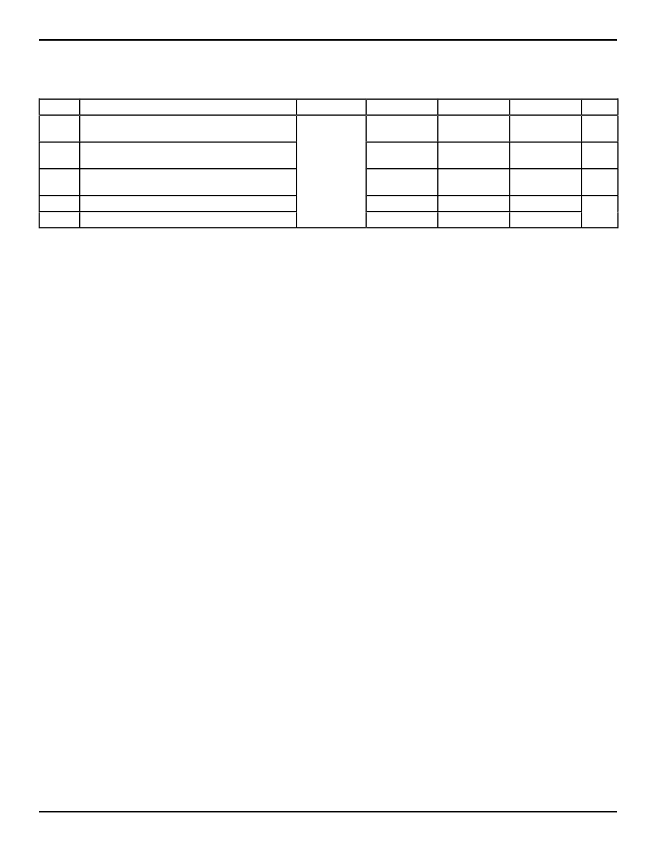
SWITHCING CHARACTERISTICS OVER OPERATING RANGE
Following Conditions Apply Unless Otherwise Specified:
Commercial: TA = –40°C to +85°C, VCC = 5.0V ±10%
Symbol
Description
Condition(1)
Min.(2)
Typ.
Max.
Unit
tPLH Data Propagation Delay
tPHL
A to B, B to A(3,4)
CL = 50pF
—
RL = 500Ω
—
0.25
ns
tPZH Switch Turn on Delay
tPZL
xOE to xBx
1.5
—
6.5
ns
tPHZ
tPLZ
|QCI|
Switch Turn off Delay
xOE to xBx
Charge Injection, Typical(5,7)
1.5
—
—
1.5
7
ns
—
pC
|QDCI| Charge Injection, Typical(6,7)
—
0.5
—
NOTES:
3615 tbl 07
1. See test circuit and waveforms.
2. Minimum limits guaranteed but not tested.
3. This parameter is guaranteed by design but not tested.
4. The bus switch contributes no propagation delay other than the RC delay of the on resistance of the switch and the load capacitance. The time constant
for the switch alone is of the order of 2.5ns for 50pF load. Since this time is constant and much smaller than the rise/fall times of typical driving signals,
it adds very little propagation delay to the system. Propagation delay on the bus switch when used in a system is determined by the driving circuit on the
driving side of the switch and its interaction with the load on the driven side.
5. Measured at switch turn off, load = 50 pF in parallel with 10 MΩ scope probe, VIN = 0.0 volts.
6. Measured at switch turn off through bus multiplexer, (e.g.- A to 1B = >A to 2B), load = 50 pF in parallel with 10 MΩ scope probe, VIN at A = 0.0 volts. Charge
injection is reduced because the injection from the turn off of the A to 1B switch is compensated by the turn on of the A to 2B switch.
7. Characterized parameter. Not 100% tested.
4
Share Link: 