HN7G02FU 데이터 시트보기 (PDF) - Toshiba
부품명
상세내역
일치하는 목록
HN7G02FU Datasheet PDF : 6 Pages
| |||
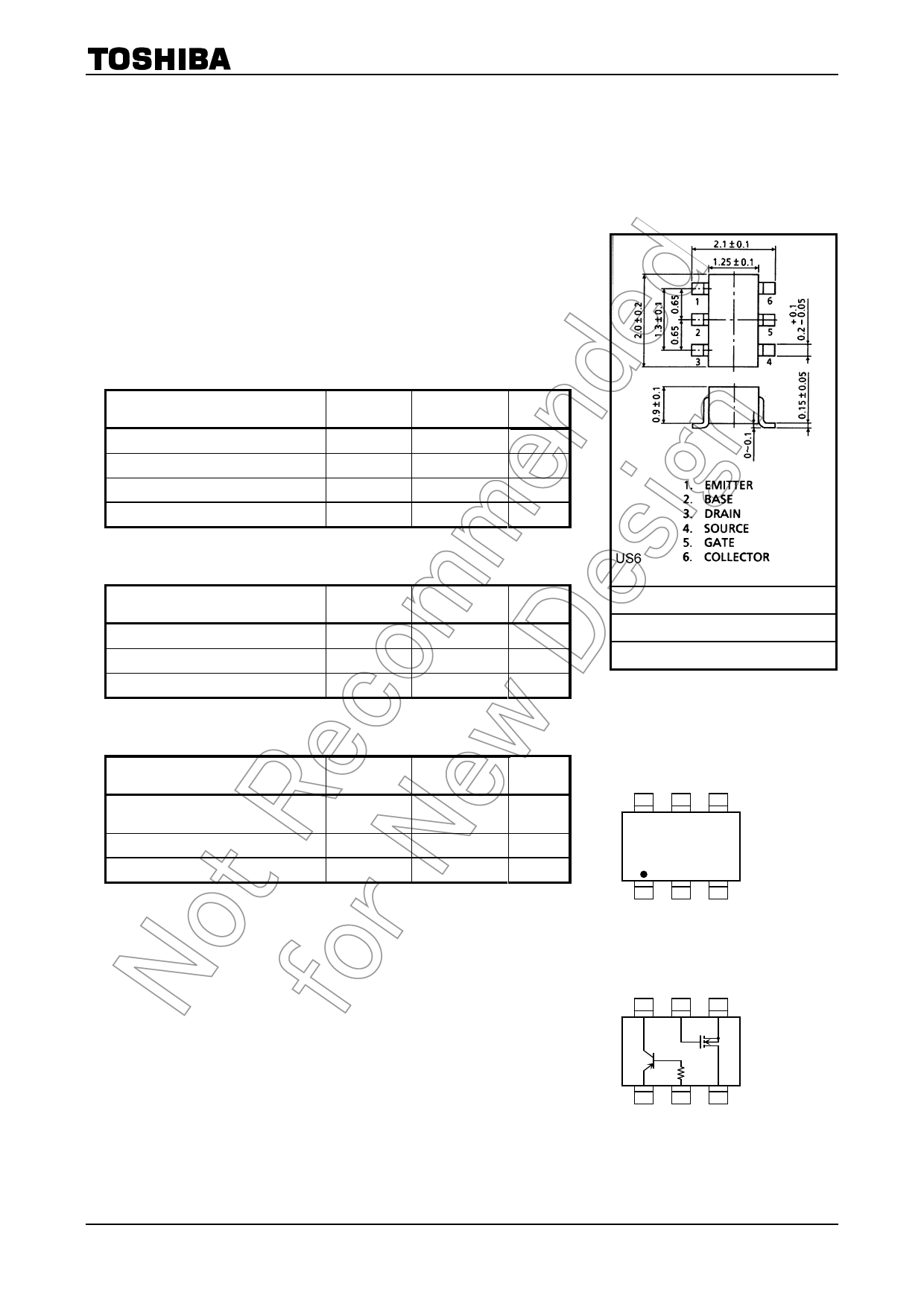
TOSHIBA Multi Chip Discrete Device
HN7G02FU
HN7G02FU
Power Management Switch Application, Inverter Circuit
Application, Driver Circuit Application and Interface
Circuit Application.
Unit: mm
Q1 (transistor): RN2110 Equivalent
Q2 (MOS-FET): 2SK1830 Equivalent
Q1 (Transistor) Absolute Maximum Ratings
(Ta = 25°C)
Characteristics
Collector-base voltage
Collector-emitter voltage
Emitter-base voltage
Collector current
Symbol
VCBO
VCEO
VEBO
IC
Rating
Unit
−50
V
−50
V
−5
V
−100
mA
Q2 (MOS-FET) Absolute Maximum Ratings (Ta = 25°C)
Characteristics
Drain-source voltage
Gate-source voltage
DC drain current
Symbol
VDS
VGSS
ID
Rating
Unit
20
V
10
V
50
mA
JEDEC
―
JEITA
―
TOSHIBA
―
Weight: g (typ.)
Q1, Q2 Common Ratings (Ta = 25°C)
Marking
Characteristics
Symbol
Rating
Unit
Collector power dissipation
PC
(Note 1)
200
mW
Junction temperature
Tj
150
°C
FT
Storage temperature range
Tstg
−55~150
°C
Note:
Using continuously under heavy loads (e.g. the application of high
temperature/current/voltage and the significant change in
temperature, etc.) may cause this product to decrease in the
reliability significantly even if the operating conditions (i.e. operating Equivalent Circuit (top view)
temperature/current/voltage, etc.) are within the absolute maximum
ratings.
654
Please design the appropriate reliability upon reviewing the Toshiba
Semiconductor Reliability Handbook (“Handling
Precautions”/“Derating Concept and Methods”) and individual
reliability data (i.e. reliability test report and estimated failure rate,
Q1
Q2
etc).
Note 1: Total rating
123
1
2007-11-01
Share Link: 