EM4095HMSO16A 데이터 시트보기 (PDF) - EM Microelectronic - MARIN SA
부품명
상세내역
일치하는 목록
EM4095HMSO16A Datasheet PDF : 10 Pages
| |||
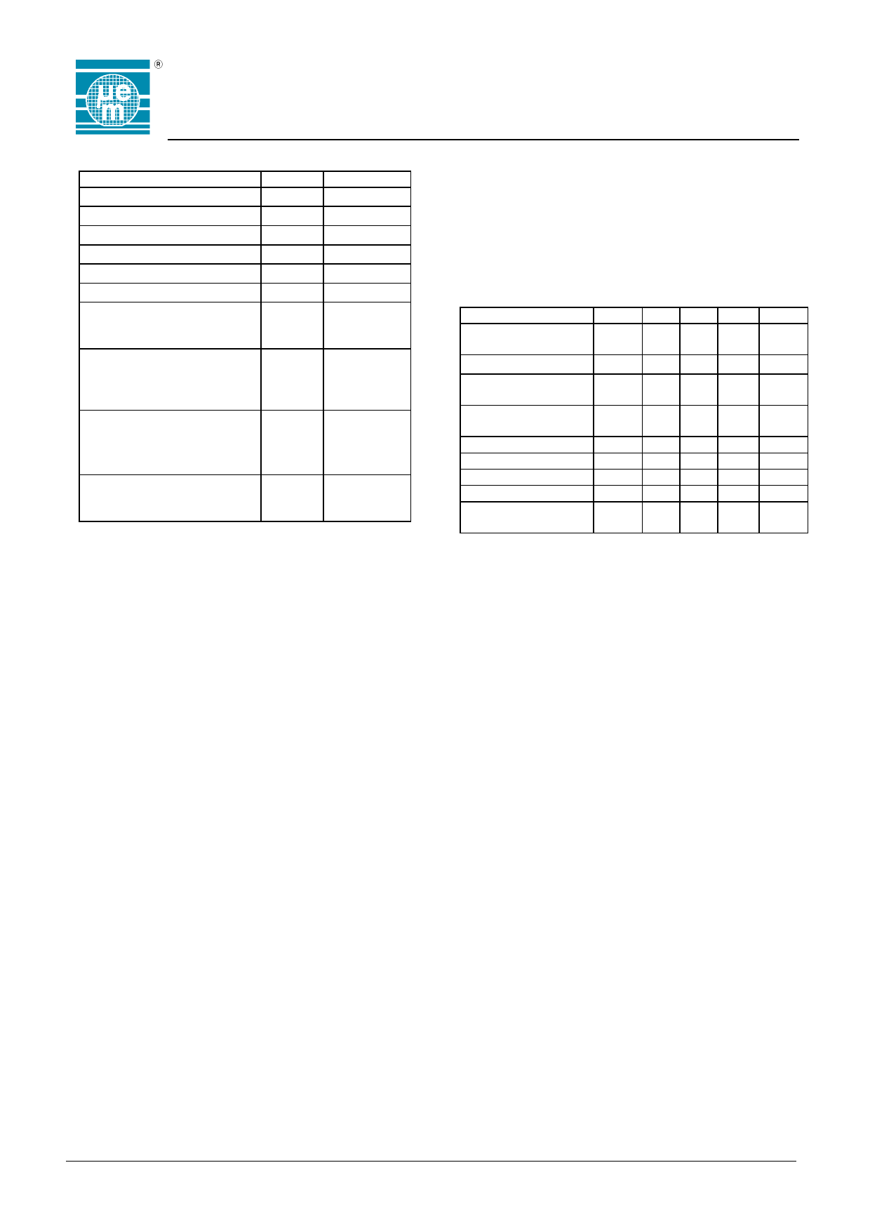
Absolute Maximum Ratings
Parameter
Storage temperature
Maximum voltage at VDD
Minimum voltage at VDD
Max. voltage other pads
Min. voltage other pads
Max. junction temperature
Electrostatic discharge max.
to MIL-STD-883C method
3015 against VSS
Electrostatic discharge max.
to MIL-STD-883C method
3015 (only for pins ANT1
and ANT2) against VSS
Maximum Input/Output
current on all pads except
VDD, VSS, DVDD, DVSS,
ANT1, ANT2, RDY/CLK
Maximum AC peak current
on ANT1 and ANT2 pads
100 kHz duty cycle 50%
Symbol
TSTO
VDDmax
VDDmin
VMAX
VMIN
TJMAX
Conditions
-55 to +150°C
VSS+6V
VSS -0.3V
VDD +0.3V
VSS -0.3V
+125°C
VESD
4000V
VESD_ANT
10000V
IIMAX
IOMAX
IANTmax
10mA
300mA
Stresses above these listed maximum ratings may cause
permanent damages to the device. Exposure beyond
specified operating conditions may affect device reliability
or cause malfunction.
EM4095
Handling Procedures
This device has built-in protection against high static
voltages or electric fields; however, anti-static precautions
must be taken as for any other CMOS component. Unless
otherwise specified, proper operation can only occur when
all terminal voltages are kept within the voltage range.
Unused inputs must always be tied to a defined logic
voltage level.
Operating Conditions
Parameter
Symb Min Typ Max Units
Operating junction TJ
-40
temperature
+110 °C
Supply voltage
VDD
4.1 5 5.5
V
Antenna circuit
resonant frequency
FRES
100 125 150
kHz
AC peak current on
ANT1 & ANT2 pads
IANT
250 mA
CFCAP
CDEC
CDC2
CAGND
Package thermal
resistor SO16
Rth j-a
* 10 *
* 100 *
* 6.80 *
100
220
69 70 71
nF
nF
nF
nF
°C/W
* ±10% tolerance capacitors should be used
** According to 1S2P JEDEC test board
Due to antenna driver current the internal junction temperature is
higher than ambient temperature. Please calculate ambient
temperature range from max. antenna current and package
Thermal Resistor. It is the user's responsibility to guarantee that
TJ remains below 110°C.
Supply voltage (VDD and DVDD pads) must be blocked by a 100nF
capacitor (to VSS) as close as possible to the chip
Copyright 2002, EM Microelectronic-Marin SA
3
www.emmicroelectronic.com
Share Link: 