EM4006F9WT11 데이터 시트보기 (PDF) - EM Microelectronic - MARIN SA
부품명
상세내역
일치하는 목록
EM4006F9WT11
EM Microelectronic - MARIN SA

EM4006F9WT11 Datasheet PDF : 10 Pages
| |||
General Description
The transponder will be activated when illuminated by a
RF field of sufficient power and at any frequency that is
compatible with its associated antenna and its internal
power supply circuit input characteristics. The chip will
Power-on-Reset itself when powered by this incoming
energy that exceeds its reset threshold. After resetting
itself the chip will start to transmit its memory contents as
a stream of Miller code. The memory contents is
transmitted by modifying the antenna matching
impedance at its internal clock rate, thereby causing
varying amounts of RF energy to be reflected from the
antenna. This impedance variation will be achieved by
connecting a modulating device across the antenna
terminals. When switched on the modulating device will
present a low impedance to the antenna. This will cause a
change in the matching of the antenna and therefore in
the amount of RF energy reflected by the transponder to
the reader. This reflected signal combines with the
transmitted signal in the receiver to yield an amplitude
modulated signal representative of the IC memory
contents. The “ON” impedance of the modulating device
needs to be comparable to about 100 Ohms to affect the
matching of the antenna and therefore its reflectivity.
The RF signal received from the transponder antenna will
serve several purposes :
• power the chip
• provide a global reset to the chip through its POR
(Power-On-Reset) function
• provide a carrier for the data transmission
• provide the input of the internal clock generation circuit
(frequency division)
EM4006
Functional Description
Output Sequence
Transmission from the transponder will be accomplished
through variation of the antenna load impedance by
switching the modulating device ON and OFF.
Output sequence is composed of cycles which are
repeated. Each cycle is composed of 82 bits Standard
Message Structure (STDMS) which is Miller coded and a
pause (LW) during which the modulating device is OFF
(see figure 6 for details of Miller code).
The pause (LW) is 9bits length.
The 82 bit STDMS consists of 1 start bit, 64 data bits, 16
CRC bits and 1 stop bit.
Start bit (1) Data(64) CRC (16) Stop bit (1) LW(9)
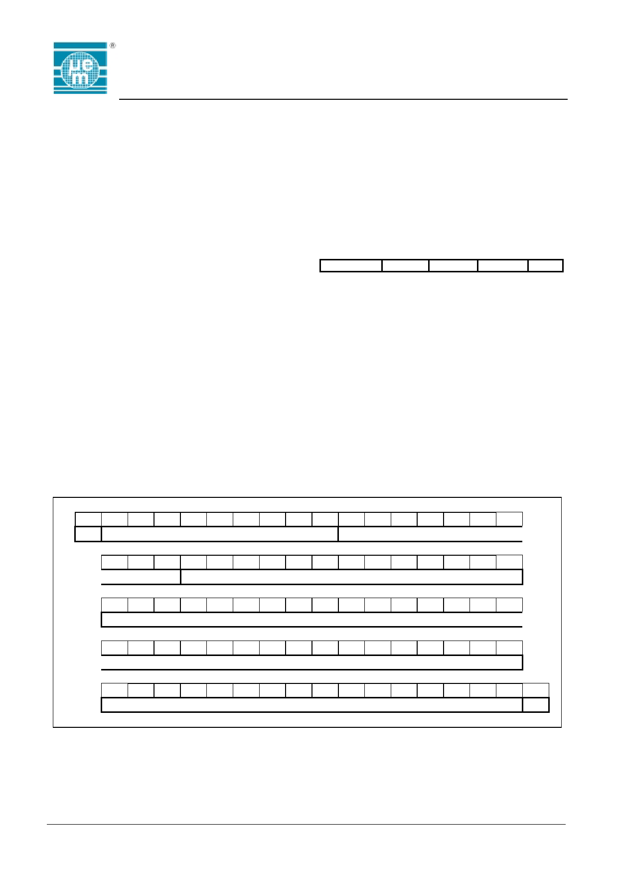
Memory organisation
As already mentioned above the 82 bits are stored in
laser programmed ROM (LROM). The 82 bits of this
LROM is partioned as followed (see Memory Map):
Factory reserved
IC name
Customer ID
ID code
CRC-CCITT
Start and stop bits
9 bits
10 bits
13 bits
32 bits
16 bits
2 bits
Memory Map
(First out)
0 1 2 3 4 5 6 7 8 9 10 11 12 13 14 15 16
Start
Factory reserved
MSB
IC Name
17 18 19 20 21 22 23 24 25 26 27 28 29 30 31 32
LSB MSB
Customer ID
LSB
33 34 35 36 37 38 39 40 41 42 43 44 45 46 47 48
MSB
ID code
49 50 51 52 53 54 55 56 57 58 59 60 61 62 63 64
ID code
LSB
65 66 67 68 69 70 71 72 73 74 75 76 77 78 79 80 81
LSB
CRC - CCITT
MSB Stop
Copyright 2001, EM Microelectronic-Marin SA
4
www.emmicroelectronic.com
Share Link: