EM4006F9WP7 데이터 시트보기 (PDF) - EM Microelectronic - MARIN SA
부품명
상세내역
일치하는 목록
EM4006F9WP7
EM Microelectronic - MARIN SA

EM4006F9WP7 Datasheet PDF : 10 Pages
| |||
EM4006
Electrical Characteristics
VDD = 2V, VSS = 0V, fC1 = 13.56MHz sine wave, VC1 = 1.0Vpp centered at (VDD - VSS)/2, Ta = 25°C
unless otherwise specified
Parameter
Symbol Test Conditions
Min. Typ. Max.
Supply Voltage
VDD
1.9
(note 1)
Units
V
Supply current
IDD
60
150
µA
Rectifier Voltage Drop
VREC
IC1C2 = 1mA, modulator switch on
VREC = (VC1-VC2) - (VDD - VSS)
1.8
V
Modulator ON DC voltage
drop (note 2)
VON1
VON2
IVDD VSS = 1mA
IVDD VSS = 10mA
1.9
2.3
2.8
V
2.4
2.8
3.3
V
Power on reset (note 3)
VR
VR - VMIN
1.2
1.4
1.7
V
0.1
0.25
0.5
V
Coil1 - Coil2 Capacitance
CRES Vcoil=100mVRMS f=10kHz
92.6 94.5 96.4
pF
Series resistance of CRES
RS
3
Ω
Power Supply Capacitor
Csup
140
pF
Note 1: Maximum voltage is defined by forcing 10 mA on C1 - C2
Note 2: Measured between VDD and VSS
Note 3: According to Figure 7
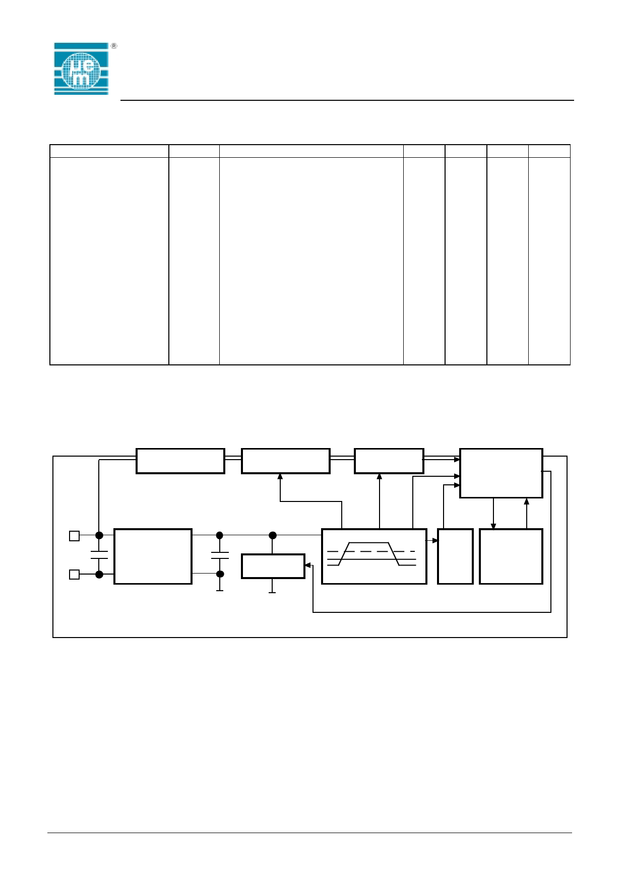
Block Diagram
Clock extractor
Divider Chain
Sequencer
Miller Code
Generator
C1
CRES
C2
AC1
+
HF Rectifier
VDD
CSUP
AC2
-
VSS
Modulator
Power Management
Power
on
Reset
LASER
ROM
Fig. 4
Copyright 2001, EM Microelectronic-Marin SA
3
www.emmicroelectronic.com
Share Link: