CS5201-1GST3 데이터 시트보기 (PDF) - Cherry semiconductor
부품명
상세내역
일치하는 목록
CS5201-1GST3 Datasheet PDF : 7 Pages
| |||
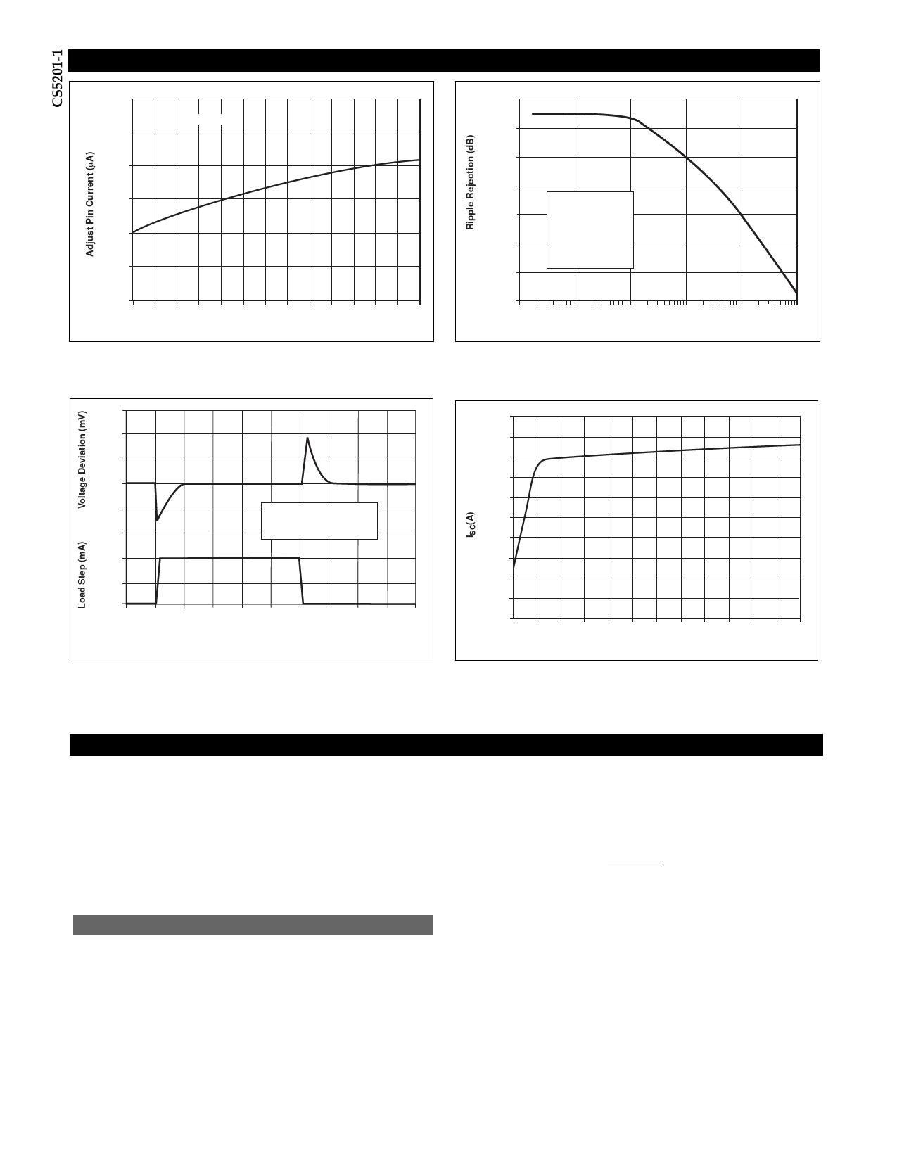
Typical Performance Characteristics: continued
70.0
IO = 10mA
65.0
60.0
55.0
50.0
45.0
40.0
0 10 20 30 40 50 60 70 80 90 100 110 120 130
Temperature (°C)
Adjust Pin Current vs. Temperature
85
75
65
55
TCASE = 25°C
45
IOUT = 1A
(VIN Ð VOUT) = 3V
35
VRIPPLE = 1.0VPP
CAdj = 0.1mF
25
15
101
102
103
104
Frequency (Hz)
Ripple Rejection vs. Frequency
105
106
200
100
0
-100
-200
1000
500
0
0
12
VOUT = 3.3V
COUT= CIN = 22mF Tantalum
CAdj= 0.1mF
3
4
5
6
Time mS
7
8
9 10
3.5
3.3
3.1
2.9
2.7
2.5
2.3
2.1
1.9
1.7
1.5
1.0
1.5
2.0
2.5
3.0
3.5
4.0
VIN - VOUT (V)
Transient Response
Short Circuit Current vs. VIN - VOUT
Applications Information
The CS5201-1 linear regulator provides adjustable volt-
ages at currents up to 1A. The regulator is protected
against overcurrent conditions and includes thermal
shutdown.
The CS5201-1 has a composite PNP-NPN output transistor
and requires an output capacitor for stability. A detailed
procedure for selecting this capacitor is included in the
Stability Considerations section.
Adjustable Operation
The CS5201-1 has an output voltage range of 1.25V to 5.5V.
An external resistor divider sets the output voltage as
shown in Figure 1. The regulator maintains a fixed 1.25V
(typical) reference between the output pin and the adjust
pin.
A resistor divider network R1 and R2 causes a fixed cur-
rent to flow to ground. This current creates a voltage
across R2 that adds to the 1.25V across R1 and sets the
overall output voltage. The adjust pin current (typically
50µA) also flows through R2 and adds a small error that
should be taken into account if precise adjustment of VOUT
is necessary.
The output voltage is set according to the formula:
( ) VOUT = VREF ´ R1 + R2 + IAdj ´ R2
R1
The term IAdj ´ R2 represents the error added by the adjust
pin current.
R1 is chosen so that the minimum load current is at least
2mA. R1 and R2 should be the same type, e.g. metal film
for best tracking over temperature. While not required, a
bypass capacitor from the adjust pin to ground will
improve ripple rejection and transient response. A 0.1µF
tantalum capacitor is recommended for Òfirst cutÓ design.
Type and value may be varied to obtain optimum perfor-
mance vs. price.
4
Share Link: 