AN80LXXRMS(2002) 데이터 시트보기 (PDF) - Panasonic Corporation
부품명
상세내역
일치하는 목록
AN80LXXRMS
(Rev.:2002)
(Rev.:2002)
Panasonic Corporation

AN80LXXRMS Datasheet PDF : 27 Pages
| |||
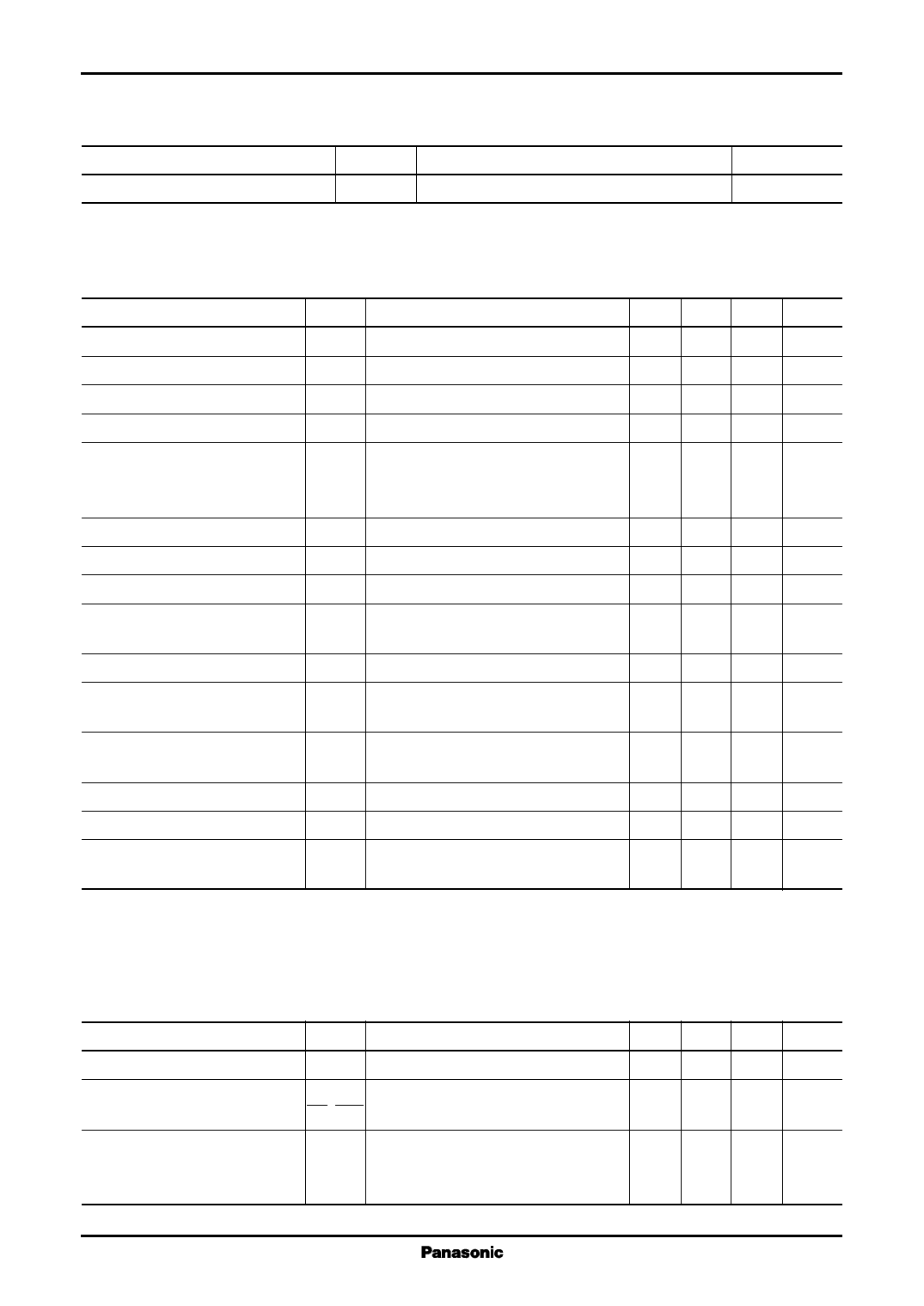
AN80LxxRMS Series
s Electrical Characteristics at Ta = 25°C (continued)
• AN80L28RMS (2.8 V type)
Unless otherwise specially provided, shorten each test time (within 10 ms) so that the test is conducted under the condition
that the drift due to the temperature increase in the chip junction part can be neglected. CIN = 0.1 µF, COUT = 10 µF
Parameter
Symbol
Conditions
Min Typ Max Unit
Output voltage
VOUT VIN = 3.8 V, IOUT = 50 mA
2.716 2.8 2.884 V
Line regulation 1
REGIN1 VIN = 3.8 V → 14.5 V, IOUT = 50 mA 10 50 mV
Line regulation 2
REGIN2 VIN = 3.8 V → 9 V, IOUT = 50 mA
5 20 mV
Load regulation *1
Peak output current *2
REGLOA VIN = 3.8 V, IOUT = 0 mA → 150 mA 50 150 mV
IPEAK VIN = 3.8 V, The output current value 180 240 mA
when VOUT decreases by 5% from its
value at IOUT = 50 mA.
Bias current under no load
IBIAS VIN = 3.8 V, IOUT = 0 mA
350 µA
Bias current fluctuation to load ∆IBIAS VIN = 3.8 V, IOUT = 0 mA → 150 mA
5
mA
Standby consumption current
ISTB VIN = 10 V, VCONT = 0 V
0.1 µA
Bias current before starting
regulation
IRUSH VIN = 2.5 V, IOUT = 0 mA
1.5 5 mA
Ripple rejection ratio
Minimum input/
output voltage difference 1
RR 1 V[rms], f = 120 Hz, IOUT = 10 mA
VDIF(min)1 VIN = 2.5 V, IOUT = 0 mA
60 68 dB
0.1 0.2 V
Minimum input/
output voltage difference 2
VDIF(min)2 VIN = 2.9 V, IOUT = 150 mA
0.4 V
Control terminal threshold high voltage VCONTH VIN = 3.8 V, IOUT = 50 mA
Control terminal threshold low voltage VCONTL VIN = 3.8 V, IOUT = 50 mA
Control terminal current
ICONT VIN = 3.8 V, IOUT = 50 mA
VCONT = 1.8 V
1.50 V
0.30
V
30 µA
Note) *1: 1.0 Ω
*2: Peak output current: The output current when the output voltage has been decreased by 5% from the value at the time
when the output current is 50 mA due to the overcurrent protection.
• Design reference data
Note) The following values are typical and not guaranteed values.
Parameter
Symbol
Conditions
Output noise voltage
VNO
Output voltage tempera- 1 · dVOUT
ture coefficient
VOUT dT
Output rise time *
tON
10 Hz ≤ f ≤ 100 kHz, IOUT = 10 mA
VIN = 3.8 V, IOUT = 0 mA
−30°C ≤ Ta ≤ +85°C
VIN = 3.8 V, IOUT = 50 mA
VCONT = 0 V → 1.8 V, CIN = 0.1 µF
COUT = 10 µF, VOUT = 90%
Note) *: Refer to "s Application Notes 3. Output rise-time characteristics".
Min Typ Max Unit
58 µV
90 ppm/°C
0.10 ms
10
SFF00008DEB
Share Link: