76132P 데이터 시트보기 (PDF) - Intersil
부품명
상세내역
일치하는 목록
76132P Datasheet PDF : 10 Pages
| |||
HUF76132P3, HUF76132S3S
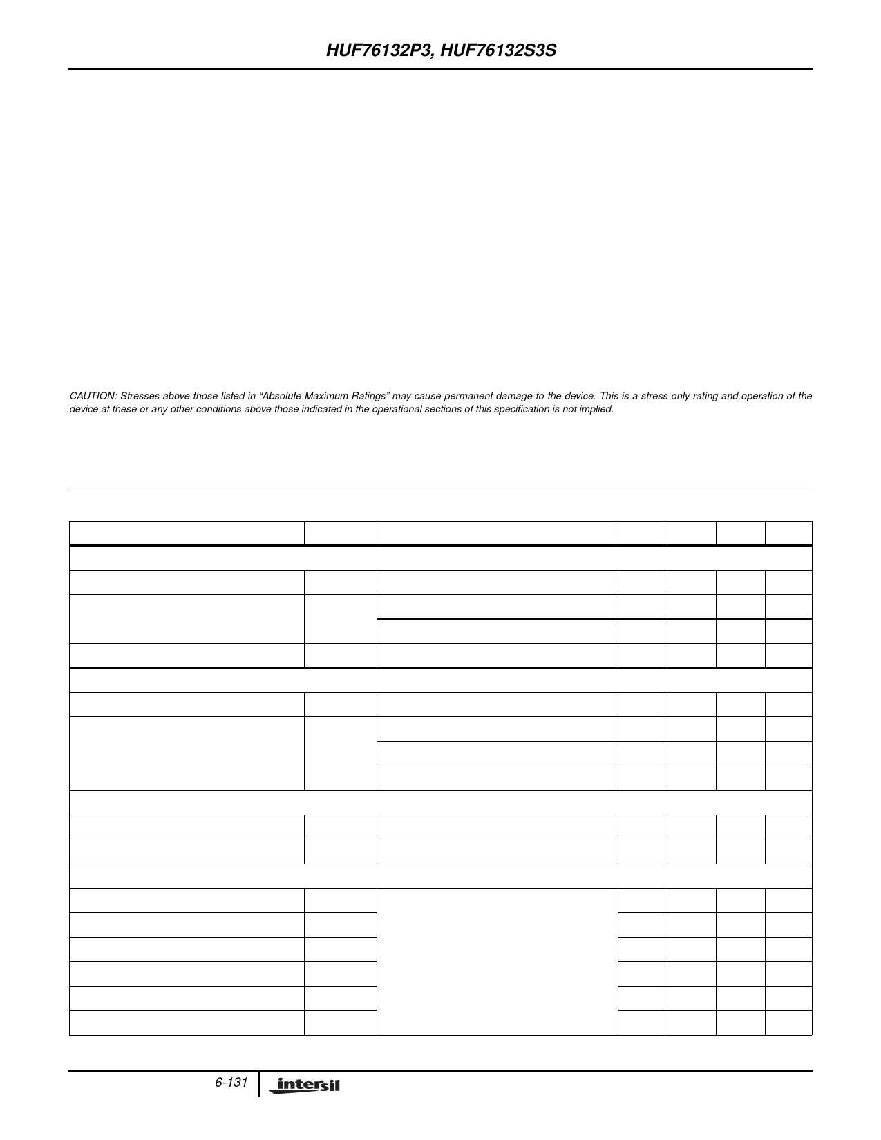
Absolute Maximum Ratings TC = 25oC, Unless Otherwise Specified
Drain to Source Voltage (Note 1). . . . . . . . . . . . . . . . . . . . . . . . . . . . . . . . . . . . . . . . . VDSS
Drain to Gate Voltage (RGS = 20kΩ) (Note 1) . . . . . . . . . . . . . . . . . . . . . . . . . . . . . . VDGR
Gate to Source Voltage . . . . . . . . . . . . . . . . . . . . . . . . . . . . . . . . . . . . . . . . . . . . . . . . . VGS
Drain Current
Continuous
Continuous
(TC
(TC
=
=
2150o0CoC, ,VVGGSS==105VV))
(Figure 2)
.........
.
.
.
.
.
.
.
.
.
.
.
.
.
.
.
.
.
.
.
.
.
.
.
.
.
.
.
.
.
.
.
.
.
.
.
.
.
.
.
.
.
.
.
.
.
.
.
.
.
.
.
.
.
.
.
.
.
.
.ID
.ID
Continuous (TC = 100oC, VGS = 4.5V) (Figure 2) . . . . . . . . . . . . . . . . . . . . . . . . . . . . .ID
Pulsed Drain Current . . . . . . . . . . . . . . . . . . . . . . . . . . . . . . . . . . . . . . . . . . . . . . . . . IDM
Pulsed Avalanche Rating. . . . . . . . . . . . . . . . . . . . . . . . . . . . . . . . . . . . . . . . . . . . . . . . EAS
Power Dissipation . . .
Derate Above 25oC
.
.
.
.
.
.
.
.
.
.
.
.
.
.
.
.
.
.
.
.
.
.
.
.
.
.
.
.
.
.
.
.
.
.
.
.
.
.
.
.
.
.
.
.
.
.
.
.
.
.
.
.
.
.
.
.
.
.
.
.
.
.
.
.
.
.
.
.
.
.
.
.
.
.
.
.
.
.
.
.
.
.
.
.
.
.
.
.
.
.
.
.
.
.
.
.
.
.
.
.
.
.
PD
..
Operating and Storage Temperature . . . . . . . . . . . . . . . . . . . . . . . . . . . . . . . . . . . TJ, TSTG
Maximum Temperature for Soldering
Leads at 0.063in (1.6mm) from Case for 10s. . . . . . . . . . . . . . . . . . . . . . . . . . . . . . . . TL
Package Body for 10s, See Techbrief 334. . . . . . . . . . . . . . . . . . . . . . . . . . . . . . . . .Tpkg
30
30
±16
75
44
41
Figure 4
Figures 6, 17, 18
120
0.97
-40 to 150
300
260
UNITS
V
V
V
A
A
A
W
W/oC
oC
oC
oC
CAUTION: Stresses above those listed in “Absolute Maximum Ratings” may cause permanent damage to the device. This is a stress only rating and operation of the
device at these or any other conditions above those indicated in the operational sections of this specification is not implied.
NOTE:
1. TJ = 25oC to 150oC.
Electrical Specifications TA = 25oC, Unless Otherwise Specified
PARAMETER
SYMBOL
TEST CONDITIONS
OFF STATE SPECIFICATIONS
Drain to Source Breakdown Voltage
Zero Gate Voltage Drain Current
Gate to Source Leakage Current
ON STATE SPECIFICATIONS
BVDSS
IDSS
IGSS
ID = 250µA, VGS = 0V (Figure 12)
VDS = 25V, VGS = 0V
VDS = 25V, VGS = 0V, TC = 150oC
VGS = ±16V
Gate to Source Threshold Voltage
Drain to Source On Resistance
THERMAL SPECIFICATIONS
VGS(TH)
rDS(ON)
VGS = VDS, ID = 250µA (Figure 11)
ID = 75A, VGS = 10V (Figure 9, 10)
ID = 44A, VGS = 5V (Figure 9)
ID = 41A, VGS = 4.5V (Figure 9)
Thermal Resistance Junction to Case
Thermal Resistance Junction to Ambient
SWITCHING SPECIFICATIONS (VGS = 4.5V)
RθJC
RθJA
(Figure 3)
TO-220, TO-262 and TO-263
Turn-On Time
Turn-On Delay Time
Rise Time
Turn-Off Delay Time
Fall Time
Turn-Off Time
tON
td(ON)
tr
td(OFF)
tf
tOFF
VDD = 15V, ID ≅ 41A,
RL = 0.366Ω, VGS = 4.5V,
RGS = 6.2Ω
(Figures 15, 21, 22)
MIN TYP MAX UNITS
30
-
-
V
-
-
1
µA
-
-
250
µA
-
-
±100 nA
1
-
3
V
-
0.0085 0.011
Ω
-
0.013 0.016
Ω
-
0.015 0.018
Ω
-
-
1.03 oC/W
-
-
62
oC/W
-
-
185
ns
-
17
-
ns
-
105
-
ns
-
33
-
ns
-
42
-
ns
-
-
113
ns
6-131
Share Link: 