2SK369-BL 데이터 시트보기 (PDF) - Toshiba
부품명
상세내역
일치하는 목록
2SK369-BL Datasheet PDF : 5 Pages
| |||
TOSHIBA Field Effect Transistor Silicon N Channel Junction Type
2SK369
2SK369
For Low Noise Audio Amplifier Applications
• Suitable for use as first stage for equalizer and MC head amplifiers.
• High |Yfs|: |Yfs| = 40 mS (typ.) (VDS = 10 V, VGS = 0, IDSS = 5 mA)
• High breakdown voltage: VGDS = −40 V (min)
• Super low noise: NF = 1.0dB (typ.)
(VDS = 10 V, ID = 5 mA, f = 1 kHz, RG = 100 Ω)
• High input impedance: IGSS = −1 nA (max) (VGS = −30 V)
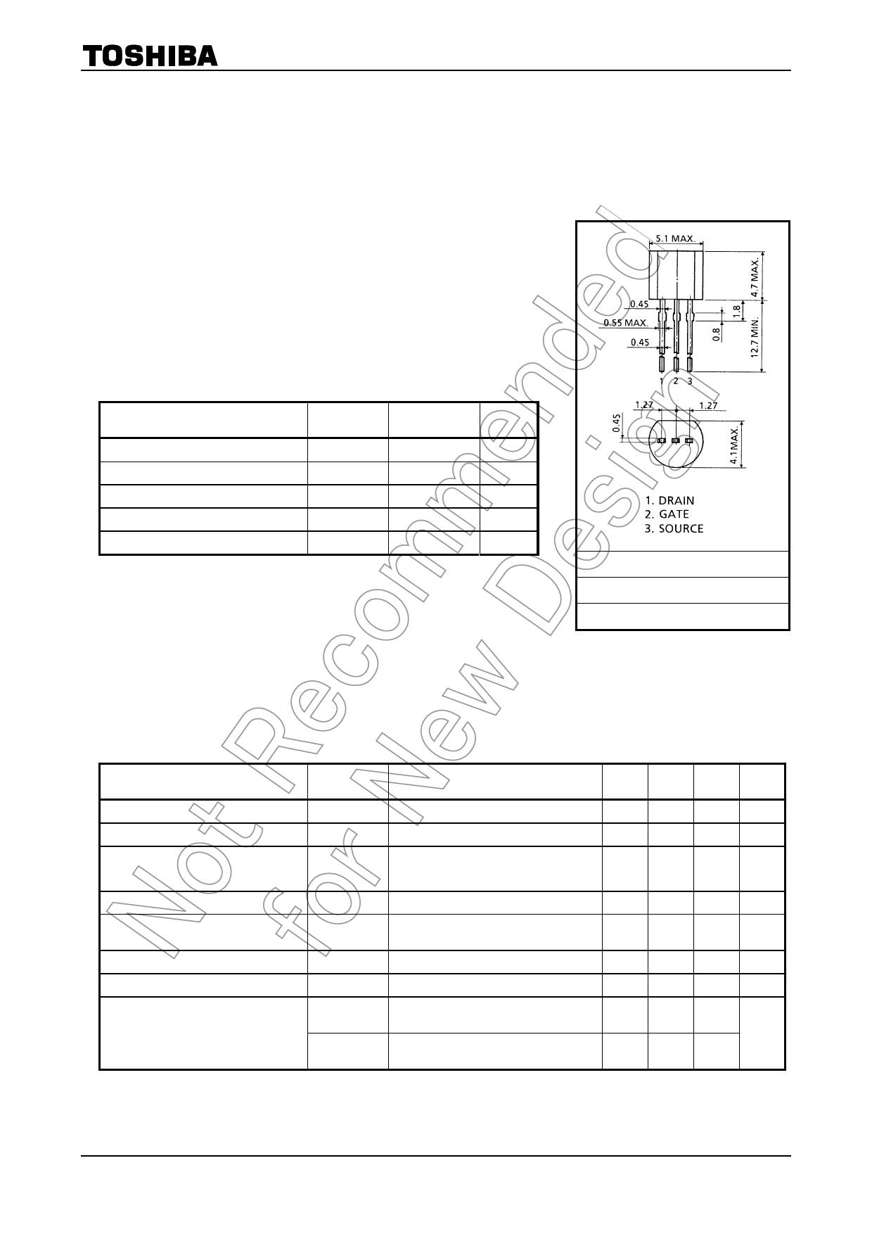
Unit: mm
Absolute Maximum Ratings (Ta = 25°C)
Characteristics
Symbol
Rating
Unit
Gate-drain voltage
VGDS
−40
V
Gate current
IG
10
mA
Drain power dissipation
PD
400
mW
Junction temperature
Tj
125
°C
Storage temperature range
Tstg
−55~125
°C
Note:
Using continuously under heavy loads (e.g. the application of
JEDEC
TO-92
high temperature/current/voltage and the significant change in
JEITA
SC-43
temperature, etc.) may cause this product to decrease in the
reliability significantly even if the operating conditions (i.e.
TOSHIBA
2-5F1D
operating temperature/current/voltage, etc.) are within the
absolute maximum ratings.
Weight: 0.21 g (typ.)
Please design the appropriate reliability upon reviewing the
Toshiba Semiconductor Reliability Handbook (“Handling Precautions”/“Derating Concept and Methods”) and
individual reliability data (i.e. reliability test report and estimated failure rate, etc).
Electrical Characteristics (Ta = 25°C)
Characteristics
Symbol
Test Condition
Min Typ. Max Unit
Gate cut-off current
Gate-drain breakdown voltage
Drain current
Gate-source cut-off voltage
Forward transfer admittance
Input capacitance
Reverse transfer capacitance
Noise figure
(Note 2)
IGSS
VGS = −30 V, VDS = 0
V (BR) GDS VDS = 0, IG = −100 μA
IDSS
VDS = 10 V, VGS = 0
(Note 1)
VGS (OFF)
⎪Yfs⎪
Ciss
Crss
NF (1)
VDS = 10 V, ID = 0.1 μA
VDS = 10 V, VGS = 0, f = 1 kHz,
(IDSS = 5 mA)
VDS = 10 V, VGS = 0, f = 1 MHz
VGD = −10 V, ID = 0, f = 1 MHz
VDS = 10 V, RG = 100 Ω, ID = 5 mA,
f = 100 Hz
NF (2)
VDS = 10 V, RG = 100 Ω, ID = 5 mA,
f = 1 kHz
⎯
⎯ −1.0 nA
−40 ⎯
⎯
V
5.0
⎯
30
mA
−0.3
⎯
−1.2
V
25
40
⎯
mS
⎯
75
⎯
pF
⎯
15
⎯
pF
⎯
5
10
dB
⎯
1
2
Note 1: IDSS classification GR: 5.0~10.0 mA, BL: 8.0~16.0 mA, V: 14.0~30.0 mA
Note 2: Use this in the low voltage region (VDS < 15 V) for low noise applications.
1
2007-11-01
Share Link: 