FM24C64VN 데이터 시트보기 (PDF) - Fairchild Semiconductor
부품명
상세내역
일치하는 목록
FM24C64VN Datasheet PDF : 13 Pages
| |||
Background Information (IIC Bus)
Extended IIC specification is an extension of Standard IIC speci-
fication to allow addressing of EEPROMs with more than 16Kbits
of memory on an IIC bus. The difference between the two
specifications is that Extended IIC specification defines two bytes
of “Array Address” information while Standard IIC specification
defines only one. All other aspects are identical between the two
specifications. Using two bytes of Array Address and 3 address
signals (A2, A1 and A0), it is now possible to address up to 4 Mbits
(28 * 28 * 23 * 8 = 4 Mbits) of memory on an IIC bus.
Note that due to format difference, it is not possible to have
peripherals which follow Standard IIC specification (e.g. 16K bit
EEPROM) and peripherals which follow Extended IIC specifica-
tion (e.g. 64K bit EEPROM) on a common IIC bus.
IIC bus allows synchronous bi-directional communication be-
tween a TRANSMITTER and a RECEIVER using a Clock signal
(SCL) and a Data signal (SDA). Additionally there are up to three
Address signals (A2, A1 and A0) which collectively serve as “chip
select signal” to a device (e.g. EEPROM) on the bus.
All communication on the IIC bus must be started with a valid
START condition (by a MASTER), followed by transmittal (by the
MASTER) of byte(s) of information (Address/Data). For every byte
of information received, the addressed RECEIVER provides a
valid ACKNOWLEDGE pulse to further continue the communica-
tion unless the RECEIVER intends to discontinue the communica-
tion. Depending on the direction of transfer (Write or Read), the
RECEIVER can be a SLAVE or the MASTER. A typical IIC
communication concludes with a STOP condition (by the MAS-
TER).
Addressing an EEPROM memory location involves sending a
command string with the following information:
[DEVICE TYPE]—[DEVICE/PAGE BLOCK SELECTION]—[R/W
BIT]—[ARRAY ADDRESS#1]—[ARRAY ADDRESS#0]
Slave Address
Slave Address is an 8-bit information consisting of a Device type
field (4bits), Device/Page block selection field (3bits) and Read/
Write bit (1bit).
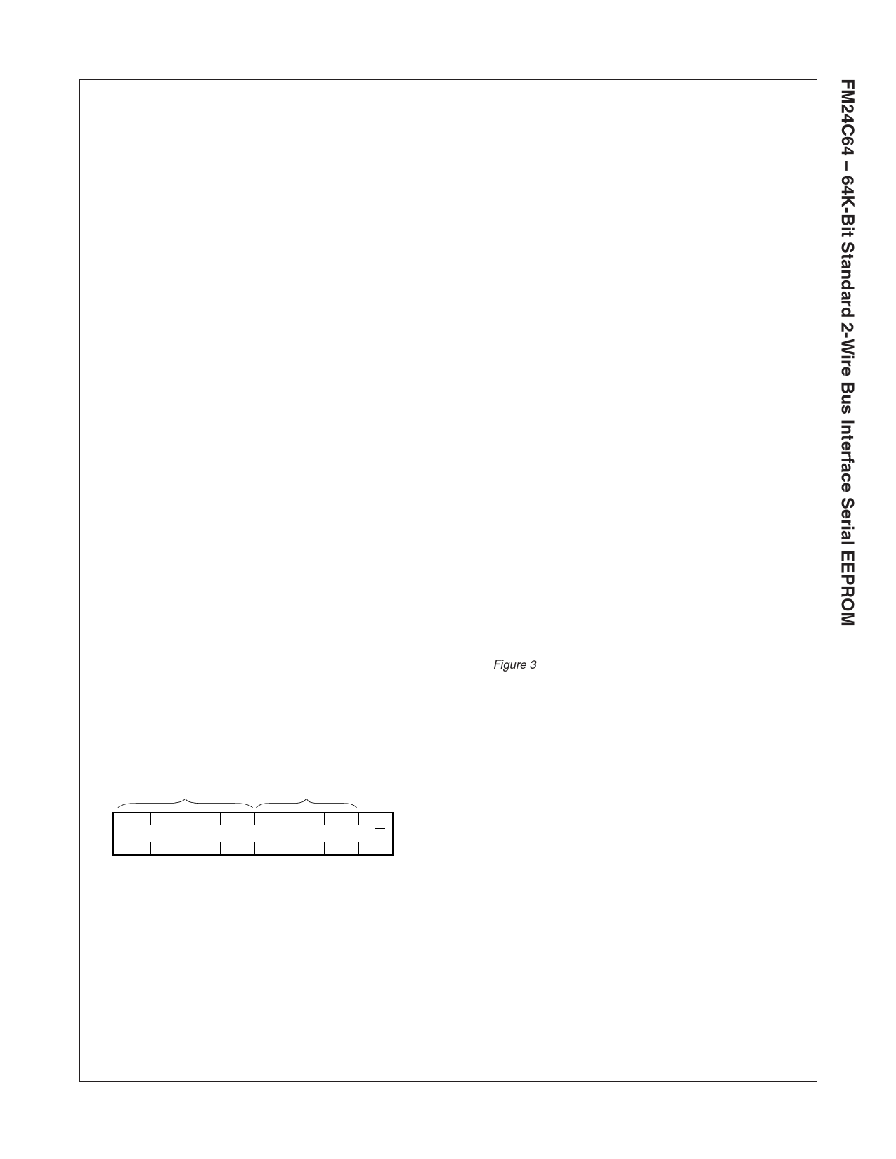
Slave Address Format
Device Type
Identifier
Device/Page Block
Selection
1
0 1 0 A2 A1 A0 R/W (LSB)
Device Type
IIC bus is designed to support a variety of devices such as RAMs,
EPROMs etc., along with EEPROMS. Hence to properly identify
various devices on the IIC bus, a 4-bit “Device Type” identifier
string is used. For EEPROMS, this 4-bit string is 1-0-1-0. Every IIC
device on the bus internally compares this 4-bit string to its own
“Device Type” string to ensure proper device selection.
Device/Page Block Selection
When multiple devices of the same type (e.g. multiple EEPROMS)
are present on the IIC bus, then the A2, A1 and A0 address
information bits are used in device selection. Every IIC device on
the bus internally compares this 3-bit string to its own physical
configuration (A2, A1 and A0 pins) to ensure proper device
selection. This comparison is in addition to the “Device Type”
comparison.
In addition to selecting an EEPROM, these 3 bits are also used to
select a “page block” within the selected EEPROM. Each page
block is 512Kbit (64 K Bytes) in size. If an EEPROM contains more
than one page bock then the selection of a page block within the
EEPROM is by using A2, A1 and A0 bits.
Read/Write Bit
Last bit of the Slave Address indicates if the intended access is
Read or Write. If the bit is "1," then the access is Read, whereas
if the bit is "0," then the access is Write.
Acknowledge
Acknowledge is an active LOW pulse on the SDA line driven by an
addressed receiver to the addressing transmitter to indicate
receipt of 8-bits of data. The receiver provides an ACK pulse for
every 8-bits of data received. This handshake mechanism is done
as follows: After transmitting 8-bits of data, the transmitter re-
leases the SDA line and waits for the ACK pulse. The addressed
receiver, if present, drives the ACK pulse on the SDA line during
the 9th clock and releases the SDA line back (to the transmitter).
Refer Figure 3.
Array Address#1
This is an 8-bit information containing the most significant 8-bits of
16-bit memory array address of a location to be selected within a
page block of the device.
Array Address#0
This is an 8-bit information containing the least significant 8-bits of
16-bit memory array address of a location to be selected within a
page block of the device.
FM24C64 Rev. C
7
www.fairchildsemi.com
Share Link: 