FDC37C93X 데이터 시트보기 (PDF) - SMSC -> Microchip
부품명
상세내역
일치하는 목록
FDC37C93X Datasheet PDF : 203 Pages
| |||
PIN NO.
94
96
97
98
99
100
102
103
104
105
106
107
108
109
110
111:118
119
120
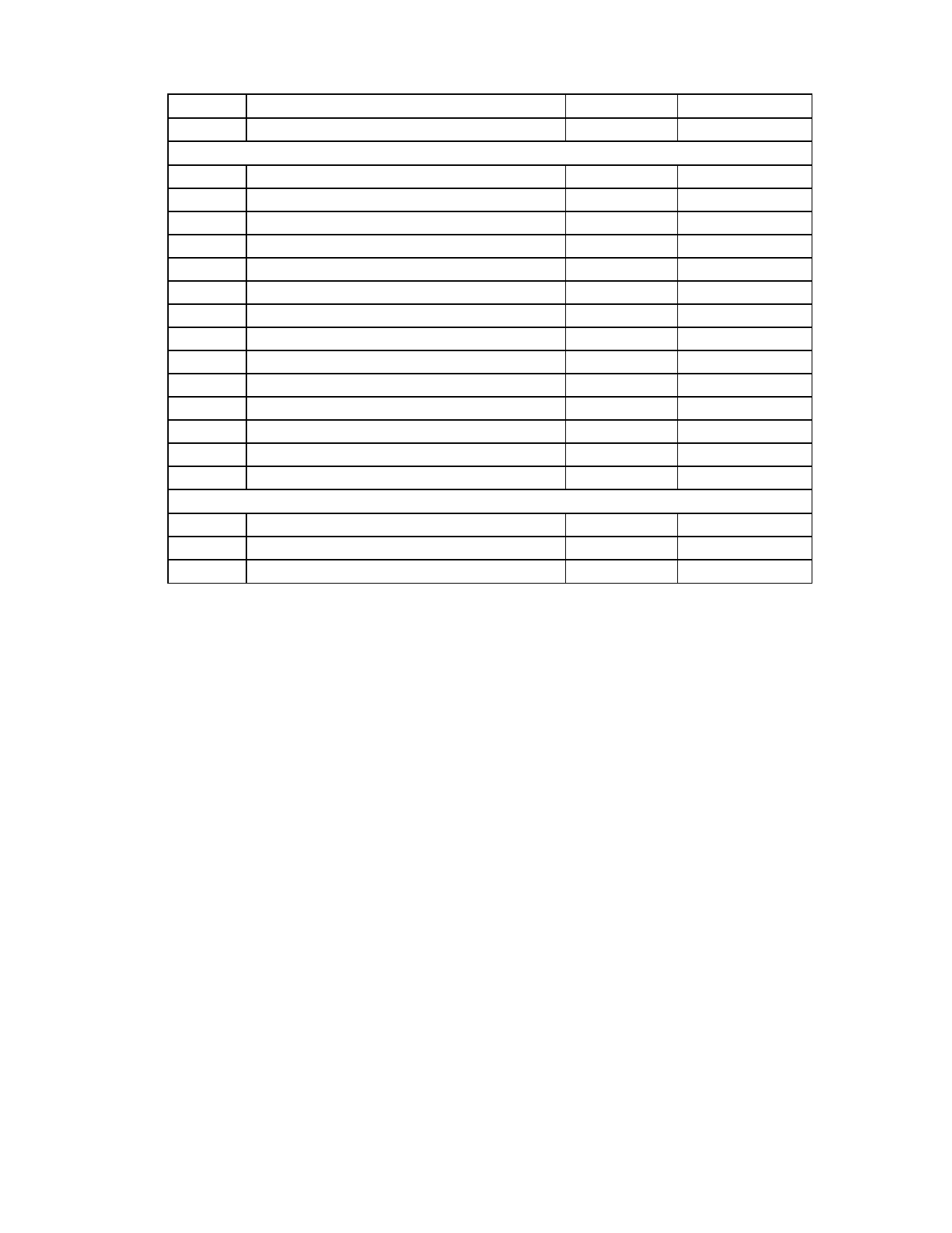
DESCRIPTION OF PIN FUNCTIONS
NAME
SYMBOL
Mouse Clock
MCLK
GENERAL PURPOSE I/O
GP I/O; IRQ in
GP10
GP I/O; IRQ in
GP11
GP I/O; WD Timer Output /IRRX
GP12
GP I/O; Power Led output /IRTX
GP13
GP I/O; GP Address Decode
GP14
GP I/O; GP Write Strobe
GP15
GP I/O; JOY Read Strobe/JOYCS
GP16
GP I/O; Joy Write Strobe
GP17
GP I/O; IDE2 Output Enable/8042 P20
GP20
GP I/O; Serial EEPROM Data In
GP21
GP I/O; Serial EEPROM Data Out
GP22
GP I/O; Serial EEPROM Clock
GP23
GP I/O; Serial EEPROM Enable
GP24
GP I/O; 8042 P21
GP25
BIOS BUFFERS
ROM Bus (I/O to the SD Bus)
RD[0:7]
ROM Chip Select (only used for ROM)
nROMCS
ROM Output Enable (DIR) (only used for ROM) nROMDIR
BUFFER TYPE
I/OD16P
I/O4
I/O4
I/O4
I/O24
I/O4
I/O4
I/O4
I/O4
I/O4
I/O4
I/O4
I/O4
I/O4
I/O4
I/O4
I
I
Note 1:
Note 2:
Note 3:
nCS -This pin is the active low chip select, it must be low for all chip accesses. For 12 bit
addressing, SA0:SA11, this input should be tied to GND. For 16 bit address qualification,
address bits SA12:SA15 can be "ORed" together and applied to this pin. If IDE2 is not
used, SA12 can be connected to nCS, pin 27 to SA13, pin 28 to SA14 and pin 29 to SA15.
nYY - The "n" as the first letter of a signal name indicates an "Active Low" signal.
nHDCS2 and nHDCS3 require a pull-up to ensure a logic high at power-up when used for
IDE2 until the Active Bit is set to 1.
8
Share Link: 