SMC91C95 데이터 시트보기 (PDF) - SMSC -> Microchip
부품명
상세내역
일치하는 목록
SMC91C95 Datasheet PDF : 139 Pages
| |||
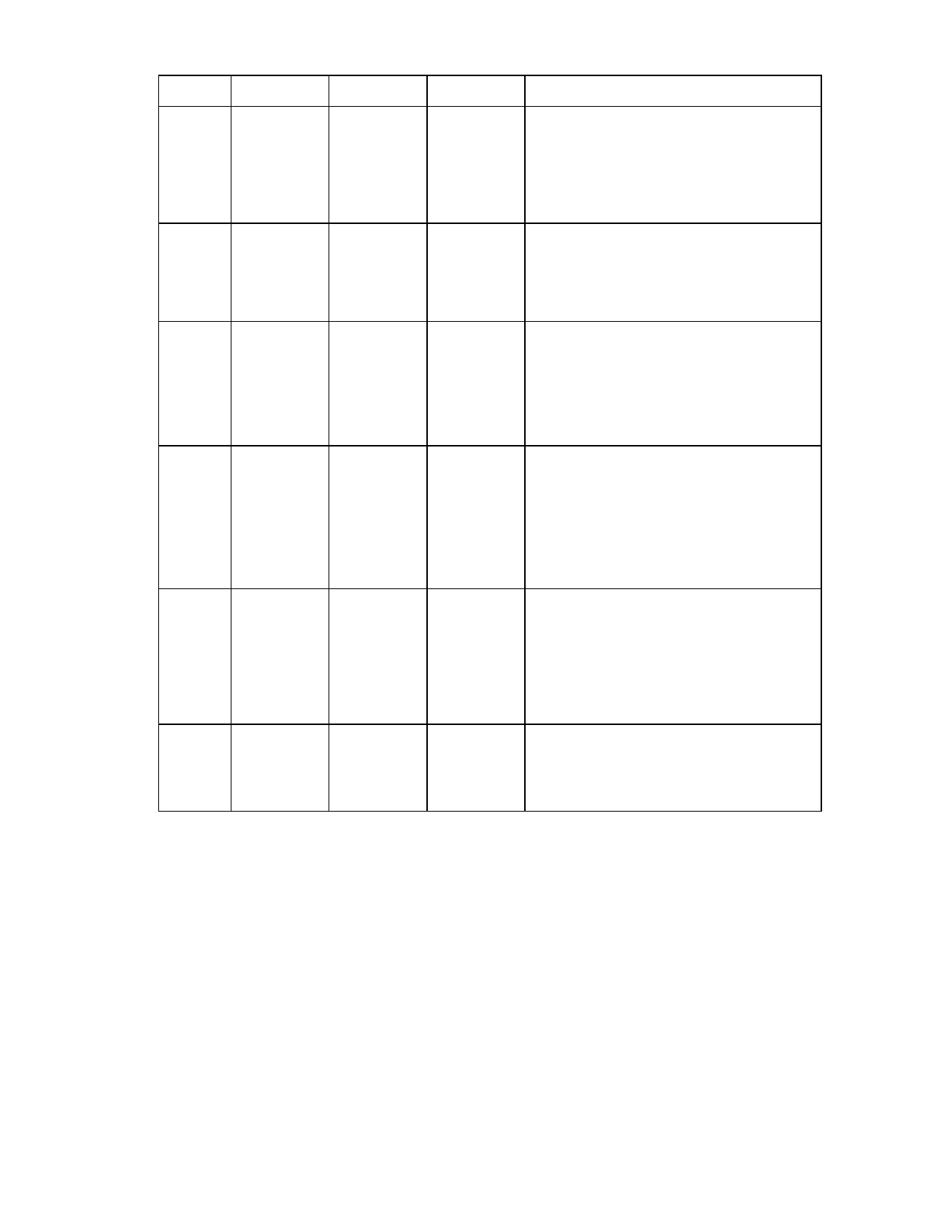
PIN NO.
NAME
81
nByte High
Enable
nCard
Enable 2
83
Ready
nWait
59, 60,
61, 63,
65, 66,
68-70,
72-74,
76-79
98
Data Bus
Reset
82
Address
Latch
nWrite
Enable
90
Interrupt
DESCRIPTION OF PIN FUNCTIONS
SYMBOL
TYPE
DESCRIPTION
nSBHE
I with pullup
ISA - Byte High Enable input. Asserted (low)
by the system to indicate a data transfer on
the upper data byte.
nCE2
PCMCIA - Card Enable 2 input. Used to
select card on odd byte accesses.
IOCHRDY
OD24 with ISA - Output. Optionally used by the
pullup
SMC91C95 to extend host cycles.
nWAIT
PCMCIA - Output. Optionally used by the
SMC91C95 to extend host cycles.
D0-D15
I/O24
Bidirectional. 16 bit data bus used to access
the SMC91C95 internal registers. The data
bus has weak internal pullups. Supports direct
connection to the system bus without external
buffering.
RESET
BALE
nWE
INTR0
IS with
pullup
IS with
pullup
O24
Input. Active high Reset. This input is not
considered active unless it is active for at least
100ns to filter narrow glitches. A POR circuit
generates an internal reset upon power up for
at least 15msec. All hardware reset
references in this spec relate to the OR
function of the POR and the RESET pin.
ISA - Input. Address strobe. For systems that
require address latching, the falling edge of
BALE latches address lines and nSBHE.
PCMCIA - Write Enable input. Used for
writing into COR and CSR registers as well as
attribute memory space.
ISA - Active high interrupt signal. The interrupt
line selection is determined by the value of
INT SEL1-0 bits in the Configuration Register.
This interrupt is tri-stated when not selected.
10
Share Link: 