W15NB50 데이터 시트보기 (PDF) - STMicroelectronics
부품명
상세내역
일치하는 목록
W15NB50 Datasheet PDF : 9 Pages
| |||
STW15NB50 - STH15NB50FI
ELECTRICAL CHARACTERISTICS (continued)
SWITCHING ON
S ymb ol
td(on)
tr
P a ra m et er
Turn-on Time
Rise Time
Qg
Total Gate Charge
Qgs Gate-Source Charge
Qgd Gate-Drain Charge
Test Conditions
VDD = 250 V ID = 7.5 A
RG = 4.7 Ω
VGS = 10 V
(see test circuit, figure 3)
VDD = 400 V ID = 15 A VGS = 10 V
Min.
Typ .
24
14
60
15
27
Max.
34
20
80
Unit
ns
ns
nC
nC
nC
SWITCHING OFF
S ymb ol
tr(Vo f f)
tf
tc
P a ra m et er
Off-voltage Rise Time
Fall Time
Cross-over Time
Test Conditions
VDD = 400 V ID = 15 A
RG = 4.7 Ω VGS = 10 V
(see test circuit, figure 5)
Min.
Typ .
15
25
35
Max.
20
33
47
Unit
ns
ns
ns
SOURCE DRAIN DIODE
S ymb ol
P a ra m et er
Test Conditions
ISD
ISDM (•)
Source-drain Current
Source-drain Current
(pulsed)
VSD (∗) Forward On Voltage
ISD = 15 A VGS = 0
trr
Reverse Recovery
Time
Qrr
Reverse Recovery
ISD = 15 A di/dt = 100 A/µs
VDD = 100 V Tj = 150 oC
(see test circuit, figure 5)
Charge
IRRM Reverse Recovery
Current
(∗) Pulsed: Pulse duration = 300 µs, duty cycle 1.5 %
(•) Pulse width limited by safe operating area
Min.
Typ .
Max.
14.6
58.4
Unit
A
A
1.6
V
680
ns
9
µC
26
A
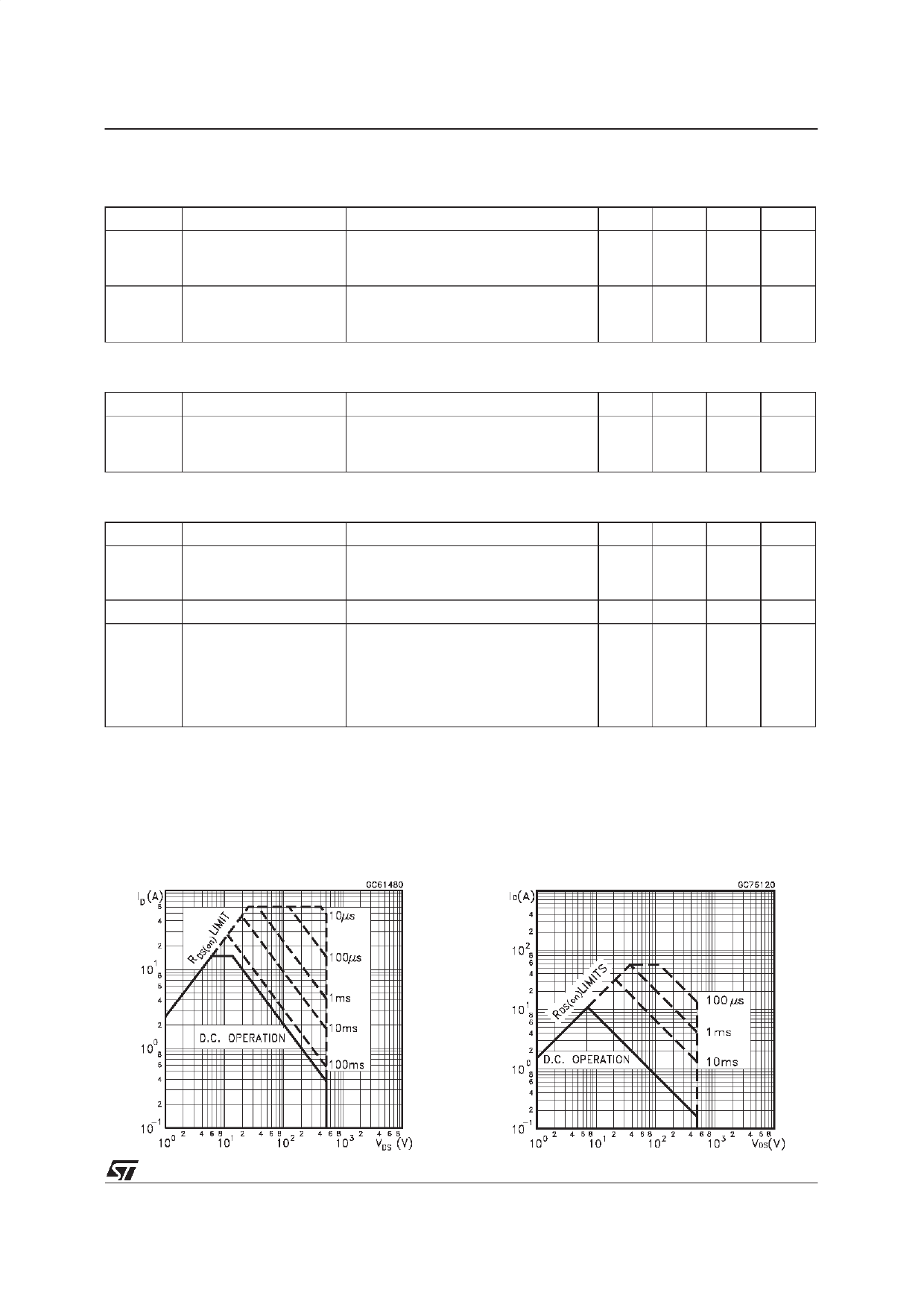
Safe Operating Area for TO-247
Safe Operating Area for ISOWATT218
3/9
Share Link: 